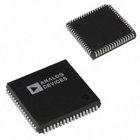
ADSP-2101BP-100 Analog Devices Inc, ADSP-2101BP-100 Datasheet - Page 10

ADSP-2101BP-100
Manufacturer Part Number
ADSP-2101BP-100
Description
IC DSP CONTROLLER 16BIT 68PLCC
Manufacturer
Analog Devices Inc
Series
ADSP-21xxr
Type
Fixed Pointr
Datasheet
1.ADSP-2115BPZ-100.pdf
(64 pages)
Specifications of ADSP-2101BP-100
Rohs Status
RoHS non-compliant
Interface
Synchronous Serial Port (SSP)
Clock Rate
25MHz
Non-volatile Memory
External
On-chip Ram
6kB
Voltage - I/o
5.00V
Voltage - Core
5.00V
Operating Temperature
-40°C ~ 85°C
Mounting Type
Surface Mount
Package / Case
68-PLCC
No. Of Bits
16 Bit
Frequency
25MHz
Supply Voltage
5V
Embedded Interface Type
Serial
No. Of Mips
25
Supply Voltage Range
4.5V To 5.5V
Lead Free Status / RoHS Status
Contains lead / RoHS non-compliant
Available stocks
Company
Part Number
Manufacturer
Quantity
Price
Company:
Part Number:
ADSP-2101BP-100
Manufacturer:
Analog Devices Inc
Quantity:
10 000
Part Number:
ADSP-2101BP-100
Manufacturer:
ADI/亚德诺
Quantity:
20 000
ADSP-21xx
The RESET input resets all internal stack pointers to the empty
stack condition, masks all interrupts, and clears the MSTAT
register. When RESET is released, the boot loading sequence is
performed (provided there is no pending bus request and the
chip is configured for booting, with MMAP = 0). The first
instruction is then fetched from internal program memory
location 0x0000.
Program Memory Interface
The on-chip program memory address bus (PMA) and on-chip
program memory data bus (PMD) are multiplexed with the on-
chip data memory buses (DMA, DMD), creating a single
external data bus and a single external address bus. The external
data bus is bidirectional and is 24 bits wide to allow instruction
fetches from external program memory. Program memory may
contain code and data.
The external address bus is 14 bits wide. For the ADSP-2101,
ADSP-2103, and ADSP-2111, these lines can directly address
up to 16K words, of which 2K are on-chip. For the ADSP-2105
and ADSP-2115, the address lines can directly address up to
15K words, of which 1K is on-chip.
1x CLOCK
CRYSTAL
or
(OPTIONAL)
(OPTIONAL)
SERIAL
DEVICE
SERIAL
DEVICE
THE TWO MSBs OF THE DATA BUS (D
BOOT MEMORY EPROM ADDRESS. THIS IS ONLY REQUIRED FOR THE 27256 AND 27512.
CLKIN
XTAL
RESET
SCLK1
RFS1 or IRQ0
TFS1 or IRQ1
DT1 or FO
DR1 or FI
FL0
FL1
FL2
CLKOUT
IRQ2
BR
BG
MMAP
SCLK0
RFS0
TFS0
DT0
DR0
HOST INTERFACE PORT
SPORT 1
SPORT 0
ADSP-2111
DATA / ADDR
Figure 5. ADSP-2111 System
CONTROL
ADDR
DATA
BMS
DMS
PMS
23-0
WR
13-0
RD
23-22
) ARE USED TO SUPPLY THE TWO MSBs OF THE
14
–10–
24
16
7
The data lines are bidirectional. The program memory select
(PMS) signal indicates accesses to program memory and can be
used as a chip select signal. The write (WR) signal indicates a
write operation and is used as a write strobe. The read (RD)
signal indicates a read operation and is used as a read strobe or
output enable signal.
The ADSP-21xx processors write data from their 16-bit
registers to 24-bit program memory using the PX register to
provide the lower eight bits. When the processor reads 16-bit
data from 24-bit program memory to a 16-bit data register, the
lower eight bits are placed in the PX register.
The program memory interface can generate 0 to 7 wait states
for external memory devices; default is to 7 wait states after
RESET.
Program Memory Maps
Program memory can be mapped in two ways, depending on the
state of the MMAP pin. Figure 6 shows the two program
memory maps for the ADSP-2101, ADSP-2103, and
ADSP-2111. Figure 8 shows the program memory maps for the
ADSP-2105 and ADSP-2115. Figures 7 and 9 show the
program memory maps for the ADSP-2161/62 and ADSP-2163/
64, respectively.
PROCESSOR
(OPTIONAL)
D
A
HOST
23-22
13-0
D
A
D
A
D
15-8
13-0
23-8
13-0
23-0
ADDR
ADDR
OE
CS
DATA
OE
WE
CS
DATA
DATA
ADDR
OE
WE
CS
PERIPHERALS
MEMORY
(OPTIONAL)
PROGRAM
MEMORY
MEMORY
(OPTIONAL)
(OPTIONAL)
BOOT
DATA
e.g. EPROM
&
27128
27256
27512
2764
REV. B


