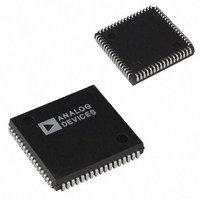
ADSP-2101BP-100 Analog Devices Inc, ADSP-2101BP-100 Datasheet - Page 19

ADSP-2101BP-100
Manufacturer Part Number
ADSP-2101BP-100
Description
IC DSP CONTROLLER 16BIT 68PLCC
Manufacturer
Analog Devices Inc
Series
ADSP-21xxr
Type
Fixed Pointr
Datasheet
1.ADSP-2115BPZ-100.pdf
(64 pages)
Specifications of ADSP-2101BP-100
Rohs Status
RoHS non-compliant
Interface
Synchronous Serial Port (SSP)
Clock Rate
25MHz
Non-volatile Memory
External
On-chip Ram
6kB
Voltage - I/o
5.00V
Voltage - Core
5.00V
Operating Temperature
-40°C ~ 85°C
Mounting Type
Surface Mount
Package / Case
68-PLCC
No. Of Bits
16 Bit
Frequency
25MHz
Supply Voltage
5V
Embedded Interface Type
Serial
No. Of Mips
25
Supply Voltage Range
4.5V To 5.5V
Lead Free Status / RoHS Status
Contains lead / RoHS non-compliant
Available stocks
Company
Part Number
Manufacturer
Quantity
Price
Company:
Part Number:
ADSP-2101BP-100
Manufacturer:
Analog Devices Inc
Quantity:
10 000
Part Number:
ADSP-2101BP-100
Manufacturer:
ADI/亚德诺
Quantity:
20 000
REV. B
SPECIFICATIONS (ADSP-2101/2105/2115/2161/2163)
POWER DISSIPATION EXAMPLE
To determine total power dissipation in a specific application,
the following equation should be applied for each output:
C = load capacitance, f = output switching frequency.
Example:
In an ADSP-2101 application where external data memory is
used and no other outputs are active, power dissipation is
calculated as follows:
Assumptions:
•
•
•
•
P
(C
Output
Address, DMS 8
Data, WR
RD
CLKOUT
Total power dissipation for this example = P
ENVIRONMENTAL CONDITIONS
Ambient Temperature Rating:
Package
PGA
PLCC
PQFP
TQFP
INT
External data memory is accessed every cycle with 50% of the
address pins switching.
External data memory writes occur every other cycle with
50% of the data pins switching.
Each address and data pin has a 10 pF total load at the pin.
The application operates at V
T
T
PD = Power Dissipation in W
CA
JA
JC
AMB
CASE
= internal power dissipation (from Figure 11).
V
= Thermal Resistance (Junction-to-Ambient)
= Thermal Resistance (Junction-to-Case)
DD
= Thermal Resistance (Case-to-Ambient)
Total Power Dissipation = P
= T
= Case Temperature in C
2
CASE
f ) is calculated for each output:
# of
Pins
9
1
1
– (PD
18 C/W
27 C/W
60 C/W
60 C/W
JA
C
10 pF
10 pF
10 pF
10 pF
C
CA
)
V
DD
DD
2
= 5.0 V and t
INT
V
5
5
5
5
2
2
2
2
DD
V
V
V
V
f
+ (C
2
9 C/W
16 C/W
18 C/W
18 C/W
JC
f
20 MHz = 40.0 mW
10 MHz = 22.5 mW
10 MHz = 2.5 mW
20 MHz = 5.0 mW
INT
V
DD
CK
+ 70.0 mW.
2
= 50 ns.
f )
70.0 mW
9 C/W
11 C/W
42 C/W
42 C/W
CA
–19–
CAPACITIVE LOADING
Figures 12 and 13 show capacitive loading characteristics for the
ADSP-2101, ADSP-2105, ADSP-2115, and ADSP-2161/2163.
Figure 13. Typical Output Valid Delay or Hold vs. Load
Capacitance, C
Figure 12. Typical Output Rise Time vs. Load Capacitance, C
(at Maximum Ambient Operating Temperature)
–1
–2
–3
8
7
6
5
4
3
2
1
0
5
4
3
2
1
0
0
0
L
(at Maximum Ambient Operating Temperature)
25
25
50
50
V
75
75
C
DD
C
L
V
L
– pF
= 4.5V
DD
– pF
100 125
100
= 4.5V
125
ADSP-21xx
150
150
175
175
L


