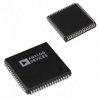
ADSP-2101BP-100 Analog Devices Inc, ADSP-2101BP-100 Datasheet - Page 8

ADSP-2101BP-100
Manufacturer Part Number
ADSP-2101BP-100
Description
IC DSP CONTROLLER 16BIT 68PLCC
Manufacturer
Analog Devices Inc
Series
ADSP-21xxr
Type
Fixed Pointr
Datasheet
1.ADSP-2115BPZ-100.pdf
(64 pages)
Specifications of ADSP-2101BP-100
Rohs Status
RoHS non-compliant
Interface
Synchronous Serial Port (SSP)
Clock Rate
25MHz
Non-volatile Memory
External
On-chip Ram
6kB
Voltage - I/o
5.00V
Voltage - Core
5.00V
Operating Temperature
-40°C ~ 85°C
Mounting Type
Surface Mount
Package / Case
68-PLCC
No. Of Bits
16 Bit
Frequency
25MHz
Supply Voltage
5V
Embedded Interface Type
Serial
No. Of Mips
25
Supply Voltage Range
4.5V To 5.5V
Lead Free Status / RoHS Status
Contains lead / RoHS non-compliant
Available stocks
Company
Part Number
Manufacturer
Quantity
Price
Company:
Part Number:
ADSP-2101BP-100
Manufacturer:
Analog Devices Inc
Quantity:
10 000
Part Number:
ADSP-2101BP-100
Manufacturer:
ADI/亚德诺
Quantity:
20 000
ADSP-21xx
A clock output signal (CLKOUT) is generated by the processor,
synchronized to the processor’s internal cycles.
Reset
The RESET signal initiates a complete reset of the ADSP-21xx.
The RESET signal must be asserted when the chip is powered
up to assure proper initialization. If the RESET signal is applied
during initial power-up, it must be held long enough to allow
the processor’s internal clock to stabilize. If RESET is activated
at any time after power-up and the input clock frequency does
not change, the processor’s internal clock continues and does
not require this stabilization time.
Pin
Name(s)
Address
Data
RESET
IRQ2
BR
BG
PMS
DMS
BMS
RD
WR
MMAP
CLKIN, XTAL
CLKOUT
V
GND
SPORT0
SPORT1
or Interrupts & Flags:
FL2–0 (ADSP-2111 Only)
Host Interface Port
(ADSP-2111 Only)
HSEL
HACK
HSIZE
BMODE
HMD0
HMD1
HRD/HRW
HWR/HDS
HD15–0/HAD15-0
HA2/ALE
HA1–0/Unused
NOTES
1
2
3
Unused data bus lines may be left floating.
BR must be tied high (to V
ADSP-2105 does not have SPORT0. (SPORT0 pins are No Connects on the ADSP-2105.)
DD
IRQ0 (RFS1)
IRQ1 (TFS1)
FI (DR1)
FO (DT1)
2
1
3
DD
) if not used.
# of
Pins
14
24
1
1
1
1
1
1
1
1
1
1
2
1
5
5
1
1
1
1
3
1
1
1
1
1
1
1
1
16
1
2
Table IV. ADSP-21xx Pin Definitions
Input /
Output
O
I/O
I
I
I
O
O
O
O
O
O
I
I
O
I/O
I/O
I
I
I
O
O
I
O
I
I
I
I
I
I
I/O
I
I
–8–
Function
Address outputs for program, data and boot memory.
Data I/O pins for program and data memories. Input only for
boot memory, with two MSBs used for boot memory addresses.
Unused data lines may be left floating.
Processor Reset Input
External Interrupt Request #2
External Bus Request Input
External Bus Grant Output
External Program Memory Select
External Data Memory Select
Boot Memory Select
External Memory Read Enable
External Memory Write Enable
Memory Map Select Input
External Clock or Quartz Crystal Input
Processor Clock Output
Power Supply Pins
Ground Pins
Serial Port 0 Pins (TFS0, RFS0, DT0, DR0, SCLK0)
Serial Port 1 Pins (TFS1, RFS1, DT1, DR1, SCLK1)
External Interrupt Request #0
External Interrupt Request #1
Flag Input Pin
Flag Output Pin
General Purpose Flag Output Pins
HIP Select Input
HIP Acknowledge Output
8/16-Bit Host Select (0 = 16-Bit, 1 = 8-Bit)
Boot Mode Select (0 = Standard EPROM Booting, 1 = HIP Booting)
Bus Strobe Select (0 = RD/WR, 1 = RW/DS)
HIP Address/Data Mode Select (0 = Separate, 1 = Multiplexed)
HIP Read Strobe or Read/Write Select
HIP Write Strobe or Host Data Strobe Select
HIP Data or HIP Data and Address
Host Address 2 Input or Address Latch Enable Input
Host Address 1 and 0 Inputs
The power-up sequence is defined as the total time required for
the crystal oscillator circuit to stabilize after a valid V
applied to the processor and for the internal phase-locked loop
(PLL) to lock onto the specific crystal frequency. A minimum of
2000 t
not, however, include the crystal oscillator start-up time).
During this power-up sequence the RESET signal should be
held low. On any subsequent resets, the RESET signal must
meet the minimum pulse width specification, t
To generate the RESET signal, use either an RC circuit with an
external Schmidt trigger or a commercially available reset IC.
(Do not use only an RC circuit.)
CK
cycles will ensure that the PLL has locked (this does
RSP
.
DD
is
REV. B


