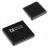
ADSP-2104BP-80 Analog Devices Inc, ADSP-2104BP-80 Datasheet - Page 12

ADSP-2104BP-80
Manufacturer Part Number
ADSP-2104BP-80
Description
IC DSP CONTROLLER 16BIT 68PLCC
Manufacturer
Analog Devices Inc
Series
ADSP-21xxr
Type
Fixed Pointr
Datasheet
1.ADSP-2104BPZ-80.pdf
(36 pages)
Specifications of ADSP-2104BP-80
Rohs Status
RoHS non-compliant
Interface
Synchronous Serial Port (SSP)
Clock Rate
20MHz
Non-volatile Memory
External
On-chip Ram
1.5kB
Voltage - I/o
5.00V
Voltage - Core
5.00V
Operating Temperature
-40°C ~ 85°C
Mounting Type
Surface Mount
Package / Case
68-PLCC
Device Core Size
16b
Architecture
Enhanced Harvard
Format
Fixed Point
Clock Freq (max)
20MHz
Mips
20
Device Input Clock Speed
20MHz
Ram Size
512Byte
Program Memory Size
8KB
Operating Temp Range
-40C to 85C
Operating Temperature Classification
Industrial
Mounting
Surface Mount
Pin Count
68
Package Type
PLCC
Lead Free Status / Rohs Status
Not Compliant
Available stocks
Company
Part Number
Manufacturer
Quantity
Price
Company:
Part Number:
ADSP-2104BP-80
Manufacturer:
AD
Quantity:
13 888
ADSP-2104/ADSP-2109–SPECIFICATIONS
RECOMMENDED OPERATING CONDITIONS
Parameter
V
T
See “Environmental Conditions” for information on thermal specifications.
ELECTRICAL CHARACTERISTICS
Parameter
V
V
V
V
V
I
I
I
I
C
C
NOTES
10
Specifications subject to change without notice.
ABSOLUTE MAXIMUM RATINGS
Supply Voltage . . . . . . . . . . . . . . . . . . . . . . . . . . –0.3 V to +7 V
Input Voltage . . . . . . . . . . . . . . . . . . . . . –0.3 V to V
Output Voltage Swing . . . . . . . . . . . . . . –0.3 V to V
Operating Temperature Range (Ambient) . . . –55ºC to +125 C
Storage Temperature Range . . . . . . . . . . . . . –65 C to +125 C
Lead Temperature (10 sec) PGA . . . . . . . . . . . . . . . . . +300 C
Lead Temperature (5 sec) PLCC, PQFP, TQFP . . . . +280 C
*Stresses greater than those listed above may cause permanent damage to the
CAUTION
ESD (electrostatic discharge) sensitive device. Electrostatic charges as high as 4000 V readily
accumulate on the human body and test equipment and can discharge without detection. Although
the ADSP-2104/ADSP-2109 processor features proprietary ESD protection circuitry to dissipate
high energy electrostatic discharges (Human Body Model), permanent damage may occur to devices
subjected to such discharges. Therefore, proper ESD precautions are recommended to avoid
performance degradation or loss of functionality. Unused devices must be stored in conductive foam
or shunts, and the foam should be discharged to the destination socket before the devices are
removed. Per method 3015 of MIL-STD-883, the ADSP-2104/ADSP-2109 processor has been
classified as Class 1 device.
1
2
3
4
5
6
7
8
9
IH
IL
OZH
OZL
device. These are stress ratings only, and functional operation of the device at these
or any other conditions greater than those indicated in the operational sections of
this specification is not implied. Exposure to absolute maximum rating conditions
for extended periods may affect device reliability.
Input-only pins: CLKIN, RESET, IRQ2, BR, MMAP, DR1, DR0.
Output pins: BG, PMS, DMS, BMS, RD, WR, A0–A13, CLKOUT, DT1, DT0.
Bidirectional pins: D0–D23, SCLK1, RFS1, TFS1, SCLK0, RFS0, TFS0.
Three-state pins: A0–A13, D0–D23, PMS, DMS, BMS, RD, WR, DT1, SCLK1, RSF1, TFS1, DT0, SCLK0, RFS0, TFS0.
Input-only pins: RESET, IRQ2, BR, MMAP, DR1, DR0.
0 V on BR, CLKIN Active (to force three-state condition).
Although specified for TTL outputs, all ADSP-2104/ADSP-2109 outputs are CMOS-compatible and will drive to V
Guaranteed but not tested.
Applies to PGA, PLCC, PQFP package types.
Output pin capacitance is the capacitive load for any three-stated output pin.
DD
IH
IH
IL
OH
OL
AMB
I
O
Hi-Level Input Voltage
Hi-Level CLKIN Voltage
Lo-Level Input Voltage
Hi-Level Output Voltage
Lo-Level Output Voltage
Hi-Level Input Current
Lo-Level Input Current
Three-State Leakage Current
Three-State Leakage Current
Input Pin Capacitance
Output Pin Capacitance
Supply Voltage
Ambient Operating Temperature
1, 8, 9
3, 5
1, 3
1
1
4, 8, 9, 10
2, 3, 7
2, 3, 7
4
4
*
Test Conditions
@ V
@ V
@ V
@ V
@ V
@ V
@ V
@ V
@ V
@ V
@ V
@ V
DD
DD
DD
DD
DD
DD
DD
DD
DD
DD
IN
IN
= 2.5 V, f
= 2.5 V, f
= max
= max
= min
= min, I
= min, I
= min, I
= max, V
= max, V
= max, V
= max, V
DD
DD
+ 0.3 V
+ 0.3 V
OH
OH
OL
IN
IN
IN
IN
IN
IN
= 2 mA
= –0.5 mA
= –100 A
= 1.0 MHz, T
= 1.0 MHz, T
= V
= 0 V
= V
= 0 V
–12–
DD
DD
6
max
max
8
6
AMB
AMB
= 25 C
= 25 C
Min
4.50
0
DD
K Grade
Min
2.0
2.2
2.4
V
and GND, assuming no dc loads.
DD
– 0.3
WARNING!
Max
5.50
+70
Max
0.8
0.4
10
10
10
10
8
8
ESD SENSITIVE DEVICE
REV. 0
Unit
Unit
V
V
V
V
V
V
pF
pF
V
A
A
A
A
C


