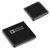
ADSP-2104BP-80 Analog Devices Inc, ADSP-2104BP-80 Datasheet - Page 3

ADSP-2104BP-80
Manufacturer Part Number
ADSP-2104BP-80
Description
IC DSP CONTROLLER 16BIT 68PLCC
Manufacturer
Analog Devices Inc
Series
ADSP-21xxr
Type
Fixed Pointr
Datasheet
1.ADSP-2104BPZ-80.pdf
(36 pages)
Specifications of ADSP-2104BP-80
Rohs Status
RoHS non-compliant
Interface
Synchronous Serial Port (SSP)
Clock Rate
20MHz
Non-volatile Memory
External
On-chip Ram
1.5kB
Voltage - I/o
5.00V
Voltage - Core
5.00V
Operating Temperature
-40°C ~ 85°C
Mounting Type
Surface Mount
Package / Case
68-PLCC
Device Core Size
16b
Architecture
Enhanced Harvard
Format
Fixed Point
Clock Freq (max)
20MHz
Mips
20
Device Input Clock Speed
20MHz
Ram Size
512Byte
Program Memory Size
8KB
Operating Temp Range
-40C to 85C
Operating Temperature Classification
Industrial
Mounting
Surface Mount
Pin Count
68
Package Type
PLCC
Lead Free Status / Rohs Status
Not Compliant
Available stocks
Company
Part Number
Manufacturer
Quantity
Price
Company:
Part Number:
ADSP-2104BP-80
Manufacturer:
AD
Quantity:
13 888
REV. 0
ARCHITECTURE OVERVIEW
Figure 1 shows a block diagram of the ADSP-2104/ADSP-2109
architecture. The processor contains three independent compu-
tational units: the ALU, the multiplier/accumulator (MAC), and
the shifter. The computational units process 16-bit data directly
and have provisions to support multiprecision computations.
The ALU performs a standard set of arithmetic and logic
operations; division primitives are also supported. The MAC
performs single-cycle multiply, multiply/add, and multiply/
subtract operations. The shifter performs logical and arithmetic
shifts, normalization, denormalization, and derive exponent
operations. The shifter can be used to efficiently implement
numeric format control including multiword floating-point
representations.
The internal result (R) bus directly connects the computational
units so that the output of any unit may be used as the input of
any unit on the next cycle.
A powerful program sequencer and two dedicated data address
generators ensure efficient use of these computational units.
The sequencer supports conditional jumps, subroutine calls,
and returns in a single cycle. With internal loop counters and
loop stacks, the ADSP-2104/ADSP-2109 executes looped code
with zero overhead—no explicit jump instructions are required
to maintain the loop. Nested loops are also supported.
Two data address generators (DAGs) provide addresses for
simultaneous dual operand fetches (from data memory and
program memory). Each DAG maintains and updates four
address pointers. Whenever the pointer is used to access data
(indirect addressing), it is post-modified by the value of one of
four modify registers. A length value may be associated with
each pointer to implement automatic modulo addressing for
GENERATOR
ADDRESS
OUTPUT REGS
INPUT REGS
DATA
#1
ALU
16
24
GENERATOR
ADDRESS
DATA
PMD BUS
DMD BUS
#2
OUTPUT REGS
14
14
INPUT REGS
PMA BUS
DMA BUS
MAC
Figure 1. ADSP-2104/ADSP-2109 Block Diagram
SEQUENCER
INSTRUCTION
PROGRAM
REGISTER
OUTPUT REGS
INPUT REGS
SHIFTER
EXCHANGE
R Bus
16
BUS
PROGRAM
MEMORY
or ROM
SRAM
–3–
TRANSMIT REG
RECEIVE REG
24
SERIAL
PORT 0
5
circular buffers. The circular buffering feature is also used by
the serial ports for automatic data transfers to (and from) on-
chip memory.
Efficient data transfer is achieved with the use of five internal
buses:
• Program Memory Address (PMA) Bus
• Program Memory Data (PMD) Bus
• Data Memory Address (DMA) Bus
• Data Memory Data (DMD) Bus
• Result (R) Bus
The two address buses (PMA, DMA) share a single external
address bus, allowing memory to be expanded off-chip, and the
two data buses (PMD, DMD) share a single external data bus.
The BMS, DMS, and PMS signals indicate which memory
space is using the external buses.
Program memory can store both instructions and data, permit-
ting the ADSP-2104/ADSP-2109 to fetch two operands in a
single cycle, one from program memory and one from data
memory. The processor can fetch an operand from on-chip
program memory and the next instruction in the same cycle.
The memory interface supports slow memories and memory-
mapped peripherals with programmable wait state generation.
External devices can gain control of the processor’s buses with
the use of the bus request/grant signals (BR, BG).
One bus grant execution mode (GO Mode) allows the ADSP-
2104/ADSP-2109 to continue running from internal memory.
A second execution mode requires the processor to halt while
buses are granted.
MEMORY
DATA
SRAM
16
COMPANDING
CIRCUITRY
PMD BUS
PMA BUS
DMA BUS
DMD BUS
TRANSMIT REG
GENERATOR
RECEIVE REG
ADDRESS
ADSP-2104/ADSP-2109
BOOT
SERIAL
PORT 1
5
TIMER
MUX
MUX
14
24
EXTERNAL
ADDRESS
BUS
EXTERNAL
DATA
BUS


