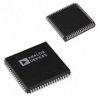
ADSP-2104BP-80 Analog Devices Inc, ADSP-2104BP-80 Datasheet - Page 5

ADSP-2104BP-80
Manufacturer Part Number
ADSP-2104BP-80
Description
IC DSP CONTROLLER 16BIT 68PLCC
Manufacturer
Analog Devices Inc
Series
ADSP-21xxr
Type
Fixed Pointr
Datasheet
1.ADSP-2104BPZ-80.pdf
(36 pages)
Specifications of ADSP-2104BP-80
Rohs Status
RoHS non-compliant
Interface
Synchronous Serial Port (SSP)
Clock Rate
20MHz
Non-volatile Memory
External
On-chip Ram
1.5kB
Voltage - I/o
5.00V
Voltage - Core
5.00V
Operating Temperature
-40°C ~ 85°C
Mounting Type
Surface Mount
Package / Case
68-PLCC
Device Core Size
16b
Architecture
Enhanced Harvard
Format
Fixed Point
Clock Freq (max)
20MHz
Mips
20
Device Input Clock Speed
20MHz
Ram Size
512Byte
Program Memory Size
8KB
Operating Temp Range
-40C to 85C
Operating Temperature Classification
Industrial
Mounting
Surface Mount
Pin Count
68
Package Type
PLCC
Lead Free Status / Rohs Status
Not Compliant
Available stocks
Company
Part Number
Manufacturer
Quantity
Price
Company:
Part Number:
ADSP-2104BP-80
Manufacturer:
AD
Quantity:
13 888
REV. 0
The interrupt control register, ICNTL, allows the external
interrupts to be set as either edge- or level-sensitive. Depending
on bit 4 in ICNTL, interrupt service routines can either be
nested (with higher priority interrupts taking precedence) or be
processed sequentially (with only one interrupt service active at
a time).
The interrupt force and clear register, IFC, is a write-only register
that contains a force bit and a clear bit for each interrupt.
When responding to an interrupt, the ASTAT, MSTAT, and
IMASK status registers are pushed onto the status stack and
the PC counter is loaded with the appropriate vector address.
The status stack is seven levels deep to allow interrupt nesting.
The stack is automatically popped when a return from the
interrupt instruction is executed.
Pin Definitions
Table II shows pin definitions for the ADSP-2104/ADSP-2109
processors. Any inputs not used must be tied to V
SYSTEM INTERFACE
Figure 3 shows a typical system for the ADSP-2104/ADSP-2109,
with two serial I/O devices, a boot EPROM, and optional external
program and data memory. A total of 14.25K words of data
memory and 14.5K words of program memory is addressable.
Pin
Name(s)
Address
Data
RESET
IRQ2
BR
BG
PMS
DMS
BMS
RD
WR
MMAP
CLKIN, XTAL
CLKOUT
V
GND
SPORT0
SPORT1
or Interrupts & Flags:
NOTES
1
2
Unused data bus lines may be left floating.
BR must be tied high (to V
DD
IRQ0 (RFS1)
IRQ1 (TFS1)
FI (DR1)
FO (DT1)
2
1
DD
) if not used.
14
# of
Pins
24
1
1
1
1
1
1
1
1
1
1
2
1
5
5
1
1
1
1
Table II. ADSP-2104/ADSP-2109 Pin Definitions
DD
Input /
Output
O
I/O
I
I
I
O
O
O
O
O
O
I
I
O
I/O
I/O
I
I
I
O
.
–5–
Function
Address outputs for program, data and boot memory.
Data I/O pins for program and data memories. Input only for
boot memory, with two MSBs used for boot memory addresses.
Unused data lines may be left floating.
Processor Reset Input
External Interrupt Request #2
External Bus Request Input
External Bus Grant Output
External Program Memory Select
External Data Memory Select
Boot Memory Select
External Memory Read Enable
External Memory Write Enable
Memory Map Select Input
External Clock or Quartz Crystal Input
Processor Clock Output
Power Supply Pins
Ground Pins
Serial Port 0 Pins (TFS0, RFS0, DT0, DR0, SCLK0)
Serial Port 1 Pins (TFS1, RFS1, DT1, DR1, SCLK1)
External Interrupt Request #0
External Interrupt Request #1
Flag Input Pin
Flag Output Pin
Programmable wait-state generation allows the processors to
easily interface to slow external memories.
The ADSP-2104/ADSP-2109 also provides either: one external
interrupt (IRQ2) and two serial ports (SPORT0, SPORT1), or
three external interrupts (IRQ2, IRQ1, IRQ0) and one serial
port (SPORT0).
Clock Signals
The ADSP-2104/ADSP-2109’s CLKIN input may be driven by
a crystal or by a TTL-compatible external clock signal. The
CLKIN input may not be halted or changed in frequency during
operation, nor operated below the specified low frequency limit.
If an external clock is used, it should be a TTL-compatible
signal running at the instruction rate. The signal should be
connected to the processor’s CLKIN input; in this case, the
XTAL input must be left unconnected.
Because the processor includes an on-chip oscillator circuit, an
external crystal may also be used. The crystal should be con-
nected across the CLKIN and XTAL pins, with two capacitors
connected as shown in Figure 2. A parallel-resonant, fundamen-
tal frequency, microprocessor-grade crystal should be used.
ADSP-2104/ADSP-2109


