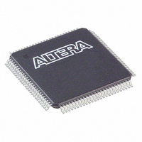
EP1K10TC100-3N Altera, EP1K10TC100-3N Datasheet - Page 17

EP1K10TC100-3N
Manufacturer Part Number
EP1K10TC100-3N
Description
IC ACEX 1K FPGA 10K 100-TQFP
Manufacturer
Altera
Series
ACEX-1K®r
Datasheet
1.EP1K10TC100-3N.pdf
(86 pages)
Specifications of EP1K10TC100-3N
Number Of Logic Elements/cells
576
Number Of Labs/clbs
72
Total Ram Bits
12288
Number Of I /o
66
Number Of Gates
56000
Voltage - Supply
2.375 V ~ 2.625 V
Mounting Type
Surface Mount
Operating Temperature
0°C ~ 85°C
Package / Case
100-TQFP, 100-VQFP
Family Name
ACEX™ 1K
Number Of Usable Gates
10000
Number Of Logic Blocks/elements
576
# I/os (max)
66
Frequency (max)
200MHz
Process Technology
CMOS
Operating Supply Voltage (typ)
2.5V
Logic Cells
576
Ram Bits
12288
Device System Gates
56000
Operating Supply Voltage (min)
2.375V
Operating Supply Voltage (max)
2.625V
Operating Temp Range
0C to 70C
Operating Temperature Classification
Commercial
Mounting
Surface Mount
Pin Count
100
Package Type
TQFP
Lead Free Status / RoHS Status
Lead free / RoHS Compliant
Other names
544-1828
EP1K10TC100-3N
EP1K10TC100-3N
Available stocks
Company
Part Number
Manufacturer
Quantity
Price
Part Number:
EP1K10TC100-3N
Manufacturer:
ALTERA/阿尔特拉
Quantity:
20 000
ACEX 1K Programmable Logic Device Family Data Sheet
Carry Chain
The carry chain provides a very fast (as low as 0.2 ns) carry-forward
function between LEs. The carry-in signal from a lower-order bit drives
forward into the higher-order bit via the carry chain, and feeds into both
the LUT and the next portion of the carry chain. This feature allows the
ACEX 1K architecture to efficiently implement high-speed counters,
adders, and comparators of arbitrary width. Carry chain logic can be
created automatically by the compiler during design processing, or
manually by the designer during design entry. Parameterized functions,
such as LPM and DesignWare functions, automatically take advantage of
carry chains.
Carry chains longer than eight LEs are automatically implemented by
linking LABs together. For enhanced fitting, a long carry chain skips
alternate LABs in a row. A carry chain longer than one LAB skips either
from even-numbered LAB to even-numbered LAB, or from odd-
numbered LAB to odd-numbered LAB. For example, the last LE of the
first LAB in a row carries to the first LE of the third LAB in the row. The
carry chain does not cross the EAB at the middle of the row. For instance,
13
in the EP1K50 device, the carry chain stops at the eighteenth LAB, and a
new carry chain begins at the nineteenth LAB.
Figure 9
shows how an n-bit full adder can be implemented in n + 1 LEs
with the carry chain. One portion of the LUT generates the sum of two bits
using the input signals and the carry-in signal; the sum is routed to the
output of the LE. The register can be bypassed for simple adders or used
for an accumulator function. Another portion of the LUT and the carry
chain logic generates the carry-out signal, which is routed directly to the
carry-in signal of the next-higher-order bit. The final carry-out signal is
routed to an LE, where it can be used as a general-purpose signal.
Altera Corporation
17


