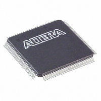
EP1K10TC100-3 Altera, EP1K10TC100-3 Datasheet - Page 50

EP1K10TC100-3
Manufacturer Part Number
EP1K10TC100-3
Description
IC ACEX 1K FPGA 10K 100-TQFP
Manufacturer
Altera
Series
ACEX-1K®r
Datasheet
1.EP1K10TC100-3N.pdf
(86 pages)
Specifications of EP1K10TC100-3
Number Of Logic Elements/cells
576
Number Of Labs/clbs
72
Total Ram Bits
12288
Number Of I /o
66
Number Of Gates
56000
Voltage - Supply
2.375 V ~ 2.625 V
Mounting Type
Surface Mount
Operating Temperature
0°C ~ 70°C
Package / Case
100-TQFP, 100-VQFP
Lead Free Status / RoHS Status
Contains lead / RoHS non-compliant
Other names
544-1027
Available stocks
Company
Part Number
Manufacturer
Quantity
Price
Part Number:
EP1K10TC100-3
Manufacturer:
ALTERA/阿尔特拉
Quantity:
20 000
Part Number:
EP1K10TC100-3N
Manufacturer:
ALTERA/阿尔特拉
Quantity:
20 000
ACEX 1K Programmable Logic Device Family Data Sheet
Figure 23. Output Drive Characteristics of ACEX 1K Devices
Timing Model
50
Typical I
Output
Current (mA)
O
30
20
10
90
80
70
60
50
40
V
The continuous, high-performance FastTrack Interconnect routing
resources ensure accurate simulation and timing analysis as well as
predictable performance. This predictable performance contrasts with
that of FPGAs, which use a segmented connection scheme and, therefore,
have an unpredictable performance.
Device performance can be estimated by following the signal path from a
source, through the interconnect, to the destination. For example, the
registered performance between two LEs on the same row can be
calculated by adding the following parameters:
The routing delay depends on the placement of the source and destination
LEs. A more complex registered path may involve multiple combinatorial
LEs between the source and destination LEs.
Timing simulation and delay prediction are available with the simulator
and Timing Analyzer, or with industry-standard EDA tools. The
Simulator offers both pre-synthesis functional simulation to evaluate logic
design accuracy and post-synthesis timing simulation with 0.1-ns
resolution. The Timing Analyzer provides point-to-point timing delay
information, setup and hold time analysis, and device-wide performance
analysis.
O
1
V
V
Room Temperature
Output Voltage (V)
CCINT
CCIO
LE register clock-to-output delay (t
Interconnect delay (t
LE look-up table delay (t
LE register setup time (t
= 2.5
= 2.5
2
V
I
OH
V
I
OL
3
Typical I
Output
Current (mA)
SAMEROW
O
SU
LUT
)
)
30
20
10
90
80
70
60
50
40
)
CO
V
O
)
1
Output Voltage (V)
2
V
V
Room Temperature
I
Altera Corporation
OL
CCINT
CCIO
3
I
OH
= 3.3
= 2.5
V
V


