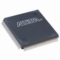
EP2C8Q208C8N Altera, EP2C8Q208C8N Datasheet - Page 100

EP2C8Q208C8N
Manufacturer Part Number
EP2C8Q208C8N
Description
IC CYCLONE II FPGA 8K 208-PQFP
Manufacturer
Altera
Series
Cyclone® IIr
Datasheet
1.EP2C5T144C8N.pdf
(168 pages)
Specifications of EP2C8Q208C8N
Number Of Logic Elements/cells
8256
Number Of Labs/clbs
516
Total Ram Bits
165888
Number Of I /o
138
Voltage - Supply
1.15 V ~ 1.25 V
Mounting Type
Surface Mount
Operating Temperature
0°C ~ 85°C
Package / Case
208-MQFP, 208-PQFP
Family Name
Cyclone® II
Number Of Logic Blocks/elements
8256
# I/os (max)
138
Frequency (max)
402.58MHz
Process Technology
90nm
Operating Supply Voltage (typ)
1.2V
Logic Cells
8256
Ram Bits
165888
Operating Supply Voltage (min)
1.15V
Operating Supply Voltage (max)
1.25V
Operating Temp Range
0C to 85C
Operating Temperature Classification
Commercial
Mounting
Surface Mount
Pin Count
208
Package Type
PQFP
Lead Free Status / RoHS Status
Lead free / RoHS Compliant
Number Of Gates
-
Lead Free Status / Rohs Status
Compliant
Other names
544-1671
Available stocks
Company
Part Number
Manufacturer
Quantity
Price
Company:
Part Number:
EP2C8Q208C8N
Manufacturer:
ALTERA
Quantity:
8
Company:
Part Number:
EP2C8Q208C8N
Manufacturer:
ALTERA
Quantity:
853
Operating Conditions
Figure 5–2. Transmitter Output Waveforms for Differential I/O Standards
Notes to
(1)
(2)
(3)
5–10
Cyclone II Device Handbook, Volume 1
LVDS
mini-LVDS
RSDS
Differential 1.5-V
HSTL class I
and II
Table 5–9. DC Characteristics for User I/O Pins Using Differential I/O Standards
I/O Standard
V
V
The p – n waveform is a function of the positive channel (p) and the negative channel (n).
OD
OCM
(3)
(2)
Figure
is the output differential voltage. V
is the output common mode voltage. V
Single-Ended Waveform
Differential Waveform (Mathematical Function of Positive and Negative Channel)
(2)
5–2:
Min
250
300
100
—
V
OD
V
Typ
—
—
—
—
OCM
(mV)
Figure 5–2
differential output standards (LVDS, mini-LVDS, RSDS, differential 1.5-V
HSTL class I and II, differential 1.8-V HSTL class I and II, differential
SSTL-2 class I and II, and differential SSTL-18 class I and II).
Table 5–9
I/O standards.
(2)
V
OD
Max
600
600
600
—
(1)
shows the DC characteristics for user I/O pins with differential
OD
shows the transmitter output waveforms for all supported
ΔV
Min Max
—
—
—
—
= |p – n|.
V
OD
OD
OCM
(mV)
(1)
50
50
—
—
= (p + n)/2.
1.125
1.125
1.125
Min
—
V
OCM
1.25
1.25
1.25
Typ
—
(V)
V
OD
1.375
1.375
1.375
Max
—
(1)
0 V
p − n (3)
Positive Channel (p) = V
Negative Channel (n) = V
Ground
V
– 0.4
Min
C C I O
—
—
—
V
Note (1)
OH
(V)
Max
—
—
—
—
Altera Corporation
(Part 1 of 2)
February 2008
OH
Min
OL
—
—
—
—
V
OL
(V)
Max
0.4
—
—
—


