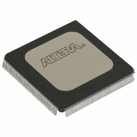
EPF10K30RI208-4 Altera, EPF10K30RI208-4 Datasheet - Page 119

EPF10K30RI208-4
Manufacturer Part Number
EPF10K30RI208-4
Description
IC FLEX 10K FPGA 30K 208-RQFP
Manufacturer
Altera
Series
FLEX-10K®r
Datasheet
1.EPF10K10ATC100-3.pdf
(128 pages)
Specifications of EPF10K30RI208-4
Number Of Logic Elements/cells
1728
Number Of Labs/clbs
216
Total Ram Bits
12288
Number Of I /o
147
Number Of Gates
69000
Voltage - Supply
4.5 V ~ 5.5 V
Mounting Type
Surface Mount
Operating Temperature
-40°C ~ 100°C
Package / Case
208-RQFP
Lead Free Status / RoHS Status
Contains lead / RoHS non-compliant
Other names
544-2233
Available stocks
Company
Part Number
Manufacturer
Quantity
Price
Company:
Part Number:
EPF10K30RI208-4
Manufacturer:
ALTERA
Quantity:
5 530
Company:
Part Number:
EPF10K30RI208-4
Manufacturer:
ALTERA
Quantity:
3 000
Part Number:
EPF10K30RI208-4
Manufacturer:
ALTERA/阿尔特拉
Quantity:
20 000
Company:
Part Number:
EPF10K30RI208-4N
Manufacturer:
VISHAY
Quantity:
1 001
Company:
Part Number:
EPF10K30RI208-4N
Manufacturer:
ALTERA
Quantity:
890
Part Number:
EPF10K30RI208-4N
Manufacturer:
XILINX/赛灵思
Quantity:
20 000
Altera Corporation
Notes to tables:
(1)
(2)
(3)
ClockLock &
ClockBoost
Timing
Parameters
t
t
t
f
t
f
t
Symbol
CLK2
CLK2
R
F
INDUTY
CLK1
CLK1
Table 113. ClockLock & ClockBoost Parameters
All timing parameters are described in
Using an LE to register the signal may provide a lower setup time.
This parameter is specified by characterization.
Input rise time
Input fall time
Input duty cycle
Input clock frequency (ClockBoost clock multiplication factor equals 1)
Input clock period (ClockBoost clock multiplication factor equals 1)
Input clock frequency (ClockBoost clock multiplication factor equals 2)
Input clock period (ClockBoost clock multiplication factor equals 2)
For the ClockLock and ClockBoost circuitry to function properly, the
incoming clock must meet certain requirements. If these specifications are
not met, the circuitry may not lock onto the incoming clock, which
generates an erroneous clock within the device. The clock generated by
the ClockLock and ClockBoost circuitry must also meet certain
specifications. If the incoming clock meets these requirements during
configuration, the ClockLock and ClockBoost circuitry will lock onto the
clock during configuration. The circuit will be ready for use immediately
after configuration.
specifications.
Figure 31. Specifications for the Incoming & Generated Clocks
Table 113
The t
nominal output clock period.
ClockLock-
Generated
Clock
I
FLEX 10K Embedded Programmable Logic Device Family Data Sheet
parameter refers to the nominal input clock period; the t
Input
Clock
Parameter
summarizes the ClockLock and ClockBoost parameters.
Tables 32
t
R
through
t
OUTDUTY
t
Figure 31
CLK1
t
F
(Part 1 of 2)
37
in this data sheet.
t
INDUTY
illustrates the incoming and generated clock
t
O
t
I
t
t
I
O +
t
INCLKSTB
t
JITTER
t
O –
Min
12.5
20
45
30
16
t
JITTER
O
parameter refers to the
t
Typ
I
f
CLKDEV
Max
62.5
33.3
55
80
50
2
2
Unit
MHz
MHz
ns
ns
ns
ns
119
%


