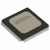
EPF10K30RC208-3 Altera, EPF10K30RC208-3 Datasheet - Page 38

EPF10K30RC208-3
Manufacturer Part Number
EPF10K30RC208-3
Description
IC FLEX 10K FPGA 30K 208-RQFP
Manufacturer
Altera
Series
FLEX-10K®r
Datasheet
1.EPF10K10ATC100-3.pdf
(128 pages)
Specifications of EPF10K30RC208-3
Number Of Logic Elements/cells
1728
Number Of Labs/clbs
216
Total Ram Bits
12288
Number Of I /o
147
Number Of Gates
69000
Voltage - Supply
4.75 V ~ 5.25 V
Mounting Type
Surface Mount
Operating Temperature
0°C ~ 85°C
Package / Case
208-RQFP
Lead Free Status / RoHS Status
Contains lead / RoHS non-compliant
Other names
544-2227
Available stocks
Company
Part Number
Manufacturer
Quantity
Price
Part Number:
EPF10K30RC208-3
Manufacturer:
ALTERA
Quantity:
20 000
Output
Configuration
38
FLEX 10K Embedded Programmable Logic Device Family Data Sheet
Figure 17. Enabling ClockLock & ClockBoost in the Same Design
To use both the ClockLock and ClockBoost circuits in the same design,
designers must use Revision C EPF10K100GC503-3DX devices and
MAX+PLUS II software versions 7.2 or higher. The die revision is
indicated by the third digit of the nine-digit code on the top side of the
device.
This section discusses the peripheral component interconnect (PCI)
pull-up clamping diode option, slew-rate control, open-drain output
option, MultiVolt I/O interface, and power sequencing for FLEX 10K
devices. The PCI pull-up clamping diode, slew-rate control, and
open-drain output options are controlled pin-by-pin via Altera logic
options. The MultiVolt I/O interface is controlled by connecting V
a different voltage than V
software via the Global Project Device Options dialog box (Assign
menu).
PCI Clamping Diodes
The EPF10K10A and EPF10K30A devices have a pull-up clamping diode
on every I/O, dedicated input, and dedicated clock pin. PCI clamping
diodes clamp the transient overshoot caused by reflected waves to the
V
can also be used to limit overshoot in other systems.
Clamping diodes are controlled on a pin-by-pin basis via a logic option in
the Altera software. When V
diode turned on can be driven by a 2.5-V or 3.3-V signal, but not a 5.0-V
signal. When V
can be driven by a 2.5-V signal, but not a 3.3-V or 5.0-V signal. However,
a clamping diode can be turned on for a subset of pins, which allows
devices to bridge between a 3.3-V PCI bus and a 5.0-V device.
CCIO
value and are required for 3.3-V PCI compliance. Clamping diodes
gclk1
CCIO
CLKLOCK
CLKLOCK
is 2.5 V, a pin that has the clamping diode turned on
CCINT
CLOCKBOOST=1
INPUT_FREQUENCY=50
CLOCKBOOST=2
INPUT_FREQUENCY=50
CCIO
. Its effect can be simulated in the Altera
a
b
is 3.3 V, a pin that has the clamping
D
D
Q
Q
Altera Corporation
aout
bout
CCIO
to


