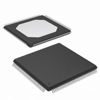
XC3S250E-4TQG144C Xilinx Inc, XC3S250E-4TQG144C Datasheet - Page 111

XC3S250E-4TQG144C
Manufacturer Part Number
XC3S250E-4TQG144C
Description
IC SPARTAN-3E FPGA 250K 144TQFP
Manufacturer
Xilinx Inc
Series
Spartan™-3Er
Datasheet
1.XC3S100E-4VQG100C.pdf
(233 pages)
Specifications of XC3S250E-4TQG144C
Number Of Logic Elements/cells
5508
Number Of Labs/clbs
612
Total Ram Bits
221184
Number Of I /o
108
Number Of Gates
250000
Voltage - Supply
1.14 V ~ 1.26 V
Mounting Type
Surface Mount
Operating Temperature
0°C ~ 85°C
Package / Case
144-LQFP
For Use With
813-1009 - MODULE USB-TO-FPGA TOOL W/MANUAL
Lead Free Status / RoHS Status
Lead free / RoHS Compliant
Other names
122-1524
Available stocks
Company
Part Number
Manufacturer
Quantity
Price
Company:
Part Number:
XC3S250E-4TQG144C
Manufacturer:
XILINX
Quantity:
2 000
Company:
Part Number:
XC3S250E-4TQG144C
Manufacturer:
XILINX
Quantity:
2 400
Company:
Part Number:
XC3S250E-4TQG144C
Manufacturer:
Xilinx Inc
Quantity:
10 000
Part Number:
XC3S250E-4TQG144C
Manufacturer:
XILINX/赛灵思
Quantity:
20 000
Part Number:
XC3S250E-4TQG144CS1
Manufacturer:
XILINX/赛灵思
Quantity:
20 000
Table 69: Spartan-3E FPGA Bitstream Generator (BitGen) Options (Continued)
Powering Spartan-3E FPGAs
For additional information, refer to the “Powering Spartan-3
Generation FPGAs” chapter in UG331.
Table 70: Spartan-3E Voltage Supplies
In a 3.3V-only application, all four V
3.3V. However, Spartan-3E FPGAs provide the ability to
bridge between different I/O voltages and standards by
applying different voltages to the V
banks. Refer to
can be intermixed within a single I/O bank.
DS312-2 (v3.8) August 26, 2009
Product Specification
CRC
Persist
Option Name
VCCO_0
VCCO_1
VCCO_2
VCCO_3
V
Supply
V
Input
CCAUX
CCINT
R
Internal core supply voltage. Supplies all internal logic functions, such as CLBs,
block RAM, and multipliers. Input to Power-On Reset (POR) circuit.
Auxiliary supply voltage. Supplies Digital Clock Managers (DCMs), differential
drivers, dedicated configuration pins, JTAG interface. Input to Power-On Reset
(POR) circuit.
Supplies the output buffers in I/O Bank 0, the bank along the top edge of the
FPGA.
Supplies the output buffers in I/O Bank 1, the bank along the right edge of the
FPGA. In
connects to the same voltage as the Flash PROM.
Supplies the output buffers in I/O Bank 2, the bank along the bottom edge of the
FPGA. Connects to the same voltage as the FPGA configuration source. Input
to Power-On Reset (POR) circuit.
Supplies the output buffers in I/O Bank 3, the bank along the left edge of the
FPGA.
I/O Banking Rules
Pins/Function
interface pins,
Configuration
Configuration
Slave mode,
SelectMAP
BPI mode,
Affected
Byte-Wide Peripheral Interface (BPI) Parallel Flash
(default)
Enable
Disable
Values
CCO
for which I/O standards
Yes
CCO
No
supplies connect to
inputs of different
Default. Enable CRC checking on the FPGA bitstream. If error detected, FPGA
asserts INIT_B Low and DONE pin stays Low.
Turn off CRC checking.
All BPI and Slave mode configuration pins are available as user-I/O after configuration.
This option is required for Readback and partial reconfiguration using the SelectMAP
interface. The SelectMAP interface pins (see
configuration and are not available as user-I/O.
Description
www.xilinx.com
Voltage Supplies
Like Spartan-3 FPGAs, Spartan-3E FPGAs have multiple
voltage supply inputs, as shown in
supply inputs for internal logic functions, V
V
supply input that powers the output buffers within the asso-
ciated I/O bank. All of the V
bank must be connected and must connect to the same
voltage.
Each I/O bank also has an separate, optional input voltage
reference supply, called V
standard that requires a voltage reference such as HSTL or
SSTL, then all V
nected to the same voltage.
CCAUX
. Each of the four I/O banks has a separate V
Description
Mode,
REF
pins within the I/O bank must be con-
Slave Parallel
REF
CCO
. If the I/O bank includes an I/O
connections to a specific I/O
Selectable, 3.3V, 2.5V,
Selectable, 3.3V, 2.5V,
Selectable, 3.3V, 2.5V,
Selectable, 3.3V, 2.5V,
Functional Description
Mode) are reserved after
Table
1.8, 1.5V, or 1.2V
1.8, 1.5V, or 1.2V
1.8, 1.5V, or 1.2V
1.8, 1.5V, or 1.2V
Nominal Supply
70. There are two
Voltage
1.2V
2.5V
CCINT
CCO
and
111


