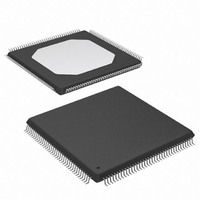
XC3S250E-4TQG144C Xilinx Inc, XC3S250E-4TQG144C Datasheet - Page 137

XC3S250E-4TQG144C
Manufacturer Part Number
XC3S250E-4TQG144C
Description
IC SPARTAN-3E FPGA 250K 144TQFP
Manufacturer
Xilinx Inc
Series
Spartan™-3Er
Datasheet
1.XC3S100E-4VQG100C.pdf
(233 pages)
Specifications of XC3S250E-4TQG144C
Number Of Logic Elements/cells
5508
Number Of Labs/clbs
612
Total Ram Bits
221184
Number Of I /o
108
Number Of Gates
250000
Voltage - Supply
1.14 V ~ 1.26 V
Mounting Type
Surface Mount
Operating Temperature
0°C ~ 85°C
Package / Case
144-LQFP
For Use With
813-1009 - MODULE USB-TO-FPGA TOOL W/MANUAL
Lead Free Status / RoHS Status
Lead free / RoHS Compliant
Other names
122-1524
Available stocks
Company
Part Number
Manufacturer
Quantity
Price
Company:
Part Number:
XC3S250E-4TQG144C
Manufacturer:
XILINX
Quantity:
2 000
Company:
Part Number:
XC3S250E-4TQG144C
Manufacturer:
XILINX
Quantity:
2 400
Company:
Part Number:
XC3S250E-4TQG144C
Manufacturer:
Xilinx Inc
Quantity:
10 000
Part Number:
XC3S250E-4TQG144C
Manufacturer:
XILINX/赛灵思
Quantity:
20 000
Part Number:
XC3S250E-4TQG144CS1
Manufacturer:
XILINX/赛灵思
Quantity:
20 000
Table 97: Recommended Number of Simultaneously
Switching Outputs per V
DS312-3 (v3.8) August 26, 2009
Product Specification
Single-Ended Standards
LVTTL
LVCMOS33
LVCMOS25
Signal Standard
(IOSTANDARD)
R
Slow
Slow
Slow
Fast
Fast
Fast
12
16
12
16
12
16
12
16
12
12
2
4
6
8
2
4
6
8
2
4
6
8
2
4
6
8
2
4
6
8
2
4
6
8
100
VQ
34
17
17
17
34
17
17
17
28
13
13
17
8
8
5
9
7
6
5
5
8
8
5
8
8
6
5
8
6
6
9
9
6
5
CCO
-GND Pair
144
TQ
20
10
10
17
20
10
10
17
16
10
16
6
6
5
9
7
6
5
5
6
6
5
8
6
6
5
8
7
6
6
9
7
6
5
Package Type
208
PQ
19
10
17
20
10
17
16
10
16
7
6
5
5
9
7
6
5
5
7
6
5
5
8
6
6
5
5
7
6
6
9
7
6
5
132
CP
52
26
26
13
13
26
13
13
52
26
26
13
13
26
13
13
42
19
19
26
13
13
6
6
6
5
6
6
6
5
9
9
6
6
FG320,
FG400,
FT256,
FG484
60
41
29
22
13
11
34
20
15
12
10
76
46
27
20
13
10
44
26
16
12
10
76
46
33
24
18
42
20
15
13
11
www.xilinx.com
9
8
Table 97: Recommended Number of Simultaneously
Switching Outputs per V
Notes:
1.
2.
3.
LVCMOS18
LVCMOS15
LVCMOS12
PCI33_3
PCI66_3
PCIX
HSTL_I_18
HSTL_III_18
SSTL18_I
SSTL2_I
Differential Standards (Number of I/O Pairs or Channels)
LVDS_25
BLVDS_25
MINI_LVDS_25
LVPECL_25
RSDS_25
DIFF_HSTL_I_18
DIFF_HSTL_IIII_18
DIFF_SSTL18_I
DIFF_SSTL2_I
The numbers in this table are recommendations that assume sound
board layout practice. This table assumes the following parasitic
factors: combined PCB trace and land inductance per V
pin of 1.0 nH, receiver capacitive load of 15 pF. Test limits are the
VIL/VIH voltage limits for the respective I/O standard.
The PQ208 results are based on physical measurements of a PQ208
package soldered to a typical printed circuit board. All other results
are based on worst-case simulation and an interpolation of the
PQ208 physical results.
If more than one signal standard is assigned to the I/Os of a given
bank, refer to XAPP689: Managing Ground Bounce in Large FPGAs
for information on how to perform weighted average SSO
calculations.
Signal Standard
(IOSTANDARD)
Slow
Slow
Slow
Fast
Fast
Fast
2
4
6
8
2
4
6
8
2
4
6
2
4
6
2
2
DC and Switching Characteristics
100
VQ
19
13
13
16
17
10
10
10
12
6
6
8
4
4
8
6
9
7
5
8
8
7
9
6
4
6
6
5
5
4
6
CCO
-GND Pair (Continued)
144
TQ
11
10
11
10
10
10
12
9
6
7
5
4
8
5
4
4
7
5
7
5
8
8
7
9
6
4
6
5
5
4
6
Package Type
Input Only
208
PQ
10
11
10
10
10
12
8
6
5
4
8
5
4
4
7
5
9
7
5
8
8
7
9
6
4
6
6
5
5
4
6
132
CP
29
19
19
13
19
13
16
10
16
13
11
16
16
15
18
12
12
12
9
9
6
6
9
9
7
5
4
8
8
7
9
CCO
FG320,
FG400,
and GND
FT256,
FG484
64
34
22
18
36
21
13
10
55
31
18
25
16
13
55
31
16
13
11
17
16
15
18
20
20
20
4
8
8
7
8
137


