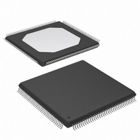
XC3S250E-4TQG144C Xilinx Inc, XC3S250E-4TQG144C Datasheet - Page 146

XC3S250E-4TQG144C
Manufacturer Part Number
XC3S250E-4TQG144C
Description
IC SPARTAN-3E FPGA 250K 144TQFP
Manufacturer
Xilinx Inc
Series
Spartan™-3Er
Datasheet
1.XC3S100E-4VQG100C.pdf
(233 pages)
Specifications of XC3S250E-4TQG144C
Number Of Logic Elements/cells
5508
Number Of Labs/clbs
612
Total Ram Bits
221184
Number Of I /o
108
Number Of Gates
250000
Voltage - Supply
1.14 V ~ 1.26 V
Mounting Type
Surface Mount
Operating Temperature
0°C ~ 85°C
Package / Case
144-LQFP
For Use With
813-1009 - MODULE USB-TO-FPGA TOOL W/MANUAL
Lead Free Status / RoHS Status
Lead free / RoHS Compliant
Other names
122-1524
Available stocks
Company
Part Number
Manufacturer
Quantity
Price
Company:
Part Number:
XC3S250E-4TQG144C
Manufacturer:
XILINX
Quantity:
2 000
Company:
Part Number:
XC3S250E-4TQG144C
Manufacturer:
XILINX
Quantity:
2 400
Company:
Part Number:
XC3S250E-4TQG144C
Manufacturer:
Xilinx Inc
Quantity:
10 000
Part Number:
XC3S250E-4TQG144C
Manufacturer:
XILINX/赛灵思
Quantity:
20 000
Part Number:
XC3S250E-4TQG144CS1
Manufacturer:
XILINX/赛灵思
Quantity:
20 000
DC and Switching Characteristics
Digital Frequency Synthesizer (DFS)
Table 106: Recommended Operating Conditions for the DFS
Table 107: Switching Characteristics for the DFS
146
Notes:
1.
2.
3.
4.
CLKOUT_PER_JITT_FX
Output Frequency Ranges
CLKOUT_FREQ_FX_LF
CLKOUT_FREQ_FX_HF
CLKOUT_FREQ_FX
Output Clock Jitter
Duty Cycle
CLKOUT_DUTY_CYCLE_FX Duty cycle precision for the CLKFX and CLKFX180
Phase Alignment
CLKOUT_PHASE_FX
CLKOUT_PHASE_FX180
Input Frequency Ranges
F
Input Clock Jitter Tolerance
CLKIN_CYC_JITT_FX_LF
CLKIN_CYC_JITT_FX_HF
CLKIN_PER_JITT_FX
CLKIN
DFS specifications apply when either of the DFS outputs (CLKFX or CLKFX180) are used.
If both DFS and DLL outputs are used on the same DCM, follow the more restrictive CLKIN_FREQ_DLL specifications in
CLKIN input jitter beyond these limits may cause the DCM to lose lock.
To support double the maximum effective FCLKIN limit, set the CLKIN_DIVIDE_BY_2 attribute to TRUE. This attribute divides the incoming
clock frequency by two as it enters the DCM.
Symbol
(4,5)
CLKIN_FREQ_FX
Symbol
(5)
(2,3)
(2)
Period jitter at the CLKFX and CLKFX180
outputs.
Frequency for the CLKFX and
CLKFX180 outputs, low frequencies
Frequency for the CLKFX and
CLKFX180 outputs, high frequencies
Frequency for the CLKFX and
CLKFX180 outputs
outputs, including the BUFGMUX and clock tree
duty-cycle distortion
Phase offset between the DFS CLKFX output and the
DLL CLK0 output when both the DFS and DLL are used
Phase offset between the DFS CLKFX180 output and the
DLL CLK0 output when both the DFS and DLL are used
(3)
Frequency for the CLKIN input
Cycle-to-cycle jitter at the
CLKIN input, based on CLKFX
output frequency
Period jitter at the CLKIN input
Description
Description
www.xilinx.com
F
F
Stepping 0
Stepping 0
Stepping 1
> 20 MHz
≤
CLKFX
CLKFX
20 MHz
CLKIN
CLKIN
< 150 MHz
> 150 MHz
XC3S1600E
XC3S1200E
XC3S100E
XC3S250E
XC3S500E
Device
All
All
All
All
All
0.200
Min
-
-
-
±[1% of
CLKFX
period
+ 100]
Min
N/A
Typ
-5
5
-
-
-
333
±300
±150
Max
Speed Grade
-5
±1
±[1% of
±[1% of
±[1% of
CLKFX
CLKFX
CLKFX
DS312-3 (v3.8) August 26, 2009
(4)
period
+ 200]
period
+ 400]
period
+ 300]
±200
Speed Grade
Max
Max
N/A
333
Note 6
0.200
Min
±[1% of
-
-
-
CLKFX
Product Specification
period
+ 100]
Min
220
Typ
5
5
-
-
-
-4
-4
Table
333
±300
±150
Max
±[1% of
±[1% of
±[1% of
CLKFX
CLKFX
CLKFX
±1
period
+ 200]
period
+ 400]
period
+ 300]
±200
Max
Max
307
307
311
(4)
90
104.
Units
MHz
Units
MHz
MHz
MHz
MHz
ps
ps
ns
ps
ps
ps
ps
ps
R


