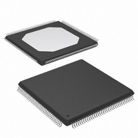
XC3S250E-4TQG144C Xilinx Inc, XC3S250E-4TQG144C Datasheet - Page 25

XC3S250E-4TQG144C
Manufacturer Part Number
XC3S250E-4TQG144C
Description
IC SPARTAN-3E FPGA 250K 144TQFP
Manufacturer
Xilinx Inc
Series
Spartan™-3Er
Datasheet
1.XC3S100E-4VQG100C.pdf
(233 pages)
Specifications of XC3S250E-4TQG144C
Number Of Logic Elements/cells
5508
Number Of Labs/clbs
612
Total Ram Bits
221184
Number Of I /o
108
Number Of Gates
250000
Voltage - Supply
1.14 V ~ 1.26 V
Mounting Type
Surface Mount
Operating Temperature
0°C ~ 85°C
Package / Case
144-LQFP
For Use With
813-1009 - MODULE USB-TO-FPGA TOOL W/MANUAL
Lead Free Status / RoHS Status
Lead free / RoHS Compliant
Other names
122-1524
Available stocks
Company
Part Number
Manufacturer
Quantity
Price
Company:
Part Number:
XC3S250E-4TQG144C
Manufacturer:
XILINX
Quantity:
2 000
Company:
Part Number:
XC3S250E-4TQG144C
Manufacturer:
XILINX
Quantity:
2 400
Company:
Part Number:
XC3S250E-4TQG144C
Manufacturer:
Xilinx Inc
Quantity:
10 000
Part Number:
XC3S250E-4TQG144C
Manufacturer:
XILINX/赛灵思
Quantity:
20 000
Part Number:
XC3S250E-4TQG144CS1
Manufacturer:
XILINX/赛灵思
Quantity:
20 000
Table 10: Slice Inputs and Outputs (Continued)
Main Logic Paths
Central to the operation of each slice are two nearly identi-
cal data paths at the top and bottom of the slice. The
description that follows uses names associated with the bot-
tom path. (The top path names appear in parentheses.) The
basic path originates at an interconnect switch matrix out-
side the CLB. See
switch matrix and the routing connections.
Four lines, F1 through F4 (or G1 through G4 on the upper
path), enter the slice and connect directly to the LUT. Once
inside the slice, the lower 4-bit path passes through a LUT
‘F’ (or ‘G’) that performs logic operations. The LUT Data out-
put, ‘D’, offers five possible paths:
1. Exit the slice via line "X" (or "Y") and return to
2. Inside the slice, "X" (or "Y") serves as an input to the
3. Control the CYMUXF (or CYMUXG) multiplexer on the
4. With the carry chain, serve as an input to the XORF (or
5. Drive the multiplexer F5MUX to implement logic
In addition to the main logic paths described above, there
are two bypass paths that enter the slice as BX and BY.
Once inside the FPGA, BX in the bottom half of the slice (or
DS312-2 (v3.8) August 26, 2009
Product Specification
CLK
SHIFTIN
SHIFTOUT
CIN
COUT
X
Y
XB
YB
XQ
YQ
Name
interconnect.
DXMUX (or DYMUX) which feeds the data input, "D", of
the FFX (or FFY) storage element. The "Q" output of
the storage element drives the line XQ (or YQ) which
exits the slice.
carry chain.
XORG) exclusive-OR gate that performs arithmetic
operations, producing a result on "X" (or "Y").
functions wider than four bits. The "D" outputs of both
the F-LUT and G-LUT serve as data inputs to this
multiplexer.
R
SLICEL/M Common
SLICEM Top
SLICEM Bottom
SLICEL/M Bottom
SLICEL/M Top
SLICEL/M Bottom
SLICEL/M Top
SLICEL/M Bottom
SLICEL/M Top
SLICEL/M Bottom
SLICEL/M Top
Interconnect
Location
for more information on the
Direction
Output
Output
Output
Output
Output
Output
Output
Output
Input
Input
Input
Shift data output from F-LUT RAM
Carry chain input
Combinatorial output
Combinatorial output
Combinatorial output from carry or F-LUT SRL16 (SLICEM)
Combinatorial output from carry or G-LUT SRL16 (SLICEM)
FFY output
FFX/Y Clock or RAM Clock (SLICEM)
Data input to G-LUT RAM
Carry chain output
FFX output
www.xilinx.com
BY in the top half) can take any of several possible
branches:
1. Bypass both the LUT and the storage element, and
2. Bypass the LUT, and then pass through a storage
3. Control the wide function multiplexer F5MUX (or
4. Via multiplexers, serve as an input to the carry chain.
5. Drive the DI input of the LUT.
6. BY can control the REV inputs of both the FFY and FFX
7. Finally, the DIG_MUX multiplexer can switch BY onto
The control inputs CLK, CE, SR, BX and BY have program-
mable polarity. The LUT inputs do not need programmable
polarity because their function can be inverted inside the
LUT.
The sections that follow provide more detail on individual
functions of the slice.
Look-Up Tables
The Look-Up Table or LUT is a RAM-based function gener-
ator and is the main resource for implementing logic func-
tions. Furthermore, the LUTs in each SLICEM pair can be
configured as Distributed RAM or a 16-bit shift register, as
described later.
Each of the two LUTs (F and G) in a slice have four logic
inputs (A1-A4) and a single output (D). Any four-variable
Boolean logic operation can be implemented in one LUT.
Functions with more inputs can be implemented by cascad-
then exit the slice as BXOUT (or BYOUT) and return to
interconnect.
element via the D input before exiting as XQ (or YQ).
FiMUX).
storage elements. See
the DIG line, which exits the slice.
Description
Storage Element
Functional Description
Functions.
25


