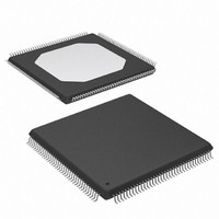
XC3S250E-4TQG144C Xilinx Inc, XC3S250E-4TQG144C Datasheet - Page 34

XC3S250E-4TQG144C
Manufacturer Part Number
XC3S250E-4TQG144C
Description
IC SPARTAN-3E FPGA 250K 144TQFP
Manufacturer
Xilinx Inc
Series
Spartan™-3Er
Datasheet
1.XC3S100E-4VQG100C.pdf
(233 pages)
Specifications of XC3S250E-4TQG144C
Number Of Logic Elements/cells
5508
Number Of Labs/clbs
612
Total Ram Bits
221184
Number Of I /o
108
Number Of Gates
250000
Voltage - Supply
1.14 V ~ 1.26 V
Mounting Type
Surface Mount
Operating Temperature
0°C ~ 85°C
Package / Case
144-LQFP
For Use With
813-1009 - MODULE USB-TO-FPGA TOOL W/MANUAL
Lead Free Status / RoHS Status
Lead free / RoHS Compliant
Other names
122-1524
Available stocks
Company
Part Number
Manufacturer
Quantity
Price
Company:
Part Number:
XC3S250E-4TQG144C
Manufacturer:
XILINX
Quantity:
2 000
Company:
Part Number:
XC3S250E-4TQG144C
Manufacturer:
XILINX
Quantity:
2 400
Company:
Part Number:
XC3S250E-4TQG144C
Manufacturer:
Xilinx Inc
Quantity:
10 000
Part Number:
XC3S250E-4TQG144C
Manufacturer:
XILINX/赛灵思
Quantity:
20 000
Part Number:
XC3S250E-4TQG144CS1
Manufacturer:
XILINX/赛灵思
Quantity:
20 000
Functional Description
The INIT attribute can be used to preload the memory with
data during FPGA configuration. The default initial contents
for RAM is all zeros. If the WE is held Low, the element can
be considered a ROM. The ROM function is possible even
in the SLICEL.
The global write enable signal, GWE, is asserted automati-
cally at the end of device configuration to enable all writable
elements. The GWE signal guarantees that the initialized
distributed RAM contents are not disturbed during the con-
figuration process.
The distributed RAM is useful for smaller amounts of mem-
ory. Larger memory requirements can use the dedicated
18Kbit RAM blocks (see
Shift Registers
For additional information, refer to the “Using Look-Up
Tables as Shift Registers (SRL16)” chapter in UG331.
It is possible to program each SLICEM LUT as a 16-bit shift
register (see
delay serial data anywhere from 1 to 16 clock cycles without
using any of the dedicated flip-flops. The resulting program-
mable delays can be used to balance the timing of data
pipelines.
The SLICEM LUTs cascade from the G-LUT to the F-LUT
through the DIFMUX (see
SHIFTOUT lines cascade a SLICEM to the SLICEM below
to form larger shift registers. The four SLICEM LUTs of a
single CLB can be combined to produce delays up to 64
clock cycles. It is also possible to combine shift registers
across more than one CLB.
34
CE (SR)
DI (BY)
A[3:0]
SHIFTIN
CLK
Figure 28: Logic Cell SRL16 Structure
Figure
4
WE
CK
A[3:0]
WS
SRLC16
WSG
SHIFT-REG
28). Used in this way, each LUT can
Block
MC15
DI
D
RAM).
Figure
SHIFTOUT
or YB
(optional)
15). SHIFTIN and
D
Q
X465_03_040203
Output
Registered
Output
www.xilinx.com
Each shift register provides a shift output MC15 for the last
bit in each LUT, in addition to providing addressable access
to any bit in the shift register through the normal D output.
The address inputs A[3:0] are the same as the distributed
RAM address lines, which come from the LUT inputs F[4:1]
or G[4:1]. At the end of the shift register, the CLB flip-flop
can be used to provide one more shift delay for the addres-
sable bit.
The shift register element is known as the SRL16 (Shift
Register LUT 16-bit), with a ‘C’ added to signify a cascade
ability (Q15 output) and ‘E’ to indicate a Clock Enable. See
Figure 29
I
The functionality of the shift register is shown in
The SRL16 shifts on the rising edge of the clock input when
the Clock Enable control is High. This shift register cannot
be initialized either during configuration or during operation
except by shifting data into it. The clock enable and clock
inputs are shared between the two LUTs in a SLICEM. The
clock enable input is automatically kept active if unused.
Table 20: SRL16 Shift Register Function
Notes:
1.
Am
Am
Am
Figure 29: SRL16 Shift Register Component with
m = 0, 1, 2, 3.
CLK
for an example of the SRLC16E component.
↑
X
Inputs
Cascade and Clock Enable
CE
0
1
CLK
CE
A0
A1
A2
A3
D
SRLC16E
D
X
D
DS312-2 (v3.8) August 26, 2009
DS312-2_43_021305
Q[Am-1]
Q[Am]
Q
Q15
Q
Product Specification
Outputs
Q[15]
Q[15]
Q15
Table
20.
R


