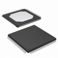
XC3S250E-4TQG144C Xilinx Inc, XC3S250E-4TQG144C Datasheet - Page 39

XC3S250E-4TQG144C
Manufacturer Part Number
XC3S250E-4TQG144C
Description
IC SPARTAN-3E FPGA 250K 144TQFP
Manufacturer
Xilinx Inc
Series
Spartan™-3Er
Datasheet
1.XC3S100E-4VQG100C.pdf
(233 pages)
Specifications of XC3S250E-4TQG144C
Number Of Logic Elements/cells
5508
Number Of Labs/clbs
612
Total Ram Bits
221184
Number Of I /o
108
Number Of Gates
250000
Voltage - Supply
1.14 V ~ 1.26 V
Mounting Type
Surface Mount
Operating Temperature
0°C ~ 85°C
Package / Case
144-LQFP
For Use With
813-1009 - MODULE USB-TO-FPGA TOOL W/MANUAL
Lead Free Status / RoHS Status
Lead free / RoHS Compliant
Other names
122-1524
Available stocks
Company
Part Number
Manufacturer
Quantity
Price
Company:
Part Number:
XC3S250E-4TQG144C
Manufacturer:
XILINX
Quantity:
2 000
Company:
Part Number:
XC3S250E-4TQG144C
Manufacturer:
XILINX
Quantity:
2 400
Company:
Part Number:
XC3S250E-4TQG144C
Manufacturer:
Xilinx Inc
Quantity:
10 000
Part Number:
XC3S250E-4TQG144C
Manufacturer:
XILINX/赛灵思
Quantity:
20 000
Part Number:
XC3S250E-4TQG144CS1
Manufacturer:
XILINX/赛灵思
Quantity:
20 000
Table 23: Block RAM Port Signals
DS312-2 (v3.8) August 26, 2009
Product Specification
Address Bus
Data Input Bus
Parity Data
Input(s)
Data Output Bus
Parity Data
Output(s)
Write Enable
Clock Enable
Set/Reset
Clock
Description
Signal
R
ADDRA
Signal
Port A
SSRA
Name
DOPA
CLKA
DIPA
WEA
DOA
ENA
DIA
ADDRB
Port B
Signal
DOPB
SSRB
Name
CLKB
DIPB
WEB
DOB
ENB
DIB
Direction
Output
Output
Input
Input
Input
Input
Input
Input
Input
www.xilinx.com
The Address Bus selects a memory location for read or write operations.
Data is written to the DO output bus from the RAM location specified by
When asserted together with EN, this input enables the writing of data to
When asserted, this input enables the CLK signal to perform read and
When asserted, this pin forces the DO output latch to the value of the
The width (w) of the port’s associated data path determines the number of
available address lines (r), as per
Whenever a port is enabled (ENA or ENB = High), address transitions
must meet the data sheet setup and hold times with respect to the port
clock (CLKA or CLKB), as shown in
must be met even if the RAM read output is of no interest.
Data at the DI input bus is written to the RAM location specified by the
address input bus (ADDR) during the active edge of the CLK input, when
the clock enable (EN) and write enable (WE) inputs are active.
It is possible to configure a port’s DI input bus width (w-p) based on
Table
port.
Parity inputs represent additional bits included in the data input path.
Although referred to herein as “parity” bits, the parity inputs and outputs
have no special functionality for generating or checking parity and can be
used as additional data bits. The number of parity bits ‘p’ included in the
DI (same as for the DO bus) depends on a port’s total data path width (w).
See
the address input bus, ADDR. See the DI signal description for DO port
width configurations.
Basic data access occurs on the active edge of the CLK when WE is
inactive and EN is active. The DO outputs mirror the data stored in the
address ADDR memory location. Data access with WE active if the
WRITE_MODE
accesses data after the write takes place.
before the write occurs. A third attribute, NO_CHANGE, latches the DO
outputs upon the assertion of WE. See
details on the WRITE_MODE attribute.
Parity outputs represent additional bits included in the data input path. The
number of parity bits ‘p’ included in the DI bus (same as for the DO bus)
depends on a port’s total data path width (w). See the DIP signal
description for configuration details.
the RAM. When WE is inactive with EN asserted, read operations are still
possible. In this case, a latch passes data from the addressed memory
location to the DO outputs.
write operations to the block RAM. When inactive, the block RAM does not
perform any read or write operations.
SRVAL attribute. It is synchronized to the CLK signal.
This input accepts the clock signal to which read and write operations are
synchronized. All associated port inputs are required to meet setup times
with respect to the clock signal’s active edge. The data output bus
responds after a clock-to-out delay referenced to the clock signal’s active
edge.
Table
22. This selection applies to both the DI and DO paths of a given
22.
attribute is set to the value: WRITE_FIRST, which
Function
Table
Table 103, page
Block RAM Data Operations
22.
READ_FIRST
Functional Description
142.This requirement
accesses data
for
39


