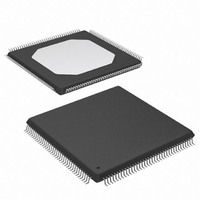
XC3S250E-4TQG144C Xilinx Inc, XC3S250E-4TQG144C Datasheet - Page 48

XC3S250E-4TQG144C
Manufacturer Part Number
XC3S250E-4TQG144C
Description
IC SPARTAN-3E FPGA 250K 144TQFP
Manufacturer
Xilinx Inc
Series
Spartan™-3Er
Datasheet
1.XC3S100E-4VQG100C.pdf
(233 pages)
Specifications of XC3S250E-4TQG144C
Number Of Logic Elements/cells
5508
Number Of Labs/clbs
612
Total Ram Bits
221184
Number Of I /o
108
Number Of Gates
250000
Voltage - Supply
1.14 V ~ 1.26 V
Mounting Type
Surface Mount
Operating Temperature
0°C ~ 85°C
Package / Case
144-LQFP
For Use With
813-1009 - MODULE USB-TO-FPGA TOOL W/MANUAL
Lead Free Status / RoHS Status
Lead free / RoHS Compliant
Other names
122-1524
Available stocks
Company
Part Number
Manufacturer
Quantity
Price
Company:
Part Number:
XC3S250E-4TQG144C
Manufacturer:
XILINX
Quantity:
2 000
Company:
Part Number:
XC3S250E-4TQG144C
Manufacturer:
XILINX
Quantity:
2 400
Company:
Part Number:
XC3S250E-4TQG144C
Manufacturer:
Xilinx Inc
Quantity:
10 000
Part Number:
XC3S250E-4TQG144C
Manufacturer:
XILINX/赛灵思
Quantity:
20 000
Part Number:
XC3S250E-4TQG144CS1
Manufacturer:
XILINX/赛灵思
Quantity:
20 000
Functional Description
Digital Clock Managers (DCMs)
For additional information, refer to the Using Digital Clock
Managers (DCMs) chapter in UG331.
Differences from the Spartan-3 Architecture
•
•
•
Overview
Spartan-3E FPGA Digital Clock Managers (DCMs) provide
flexible, complete control over clock frequency, phase shift
and skew. To accomplish this, the DCM employs a
Delay-Locked Loop (DLL), a fully digital control system that
uses feedback to maintain clock signal characteristics with a
high degree of precision despite normal variations in oper-
ating temperature and voltage. This section provides a fun-
damental description of the DCM.
The XC3S100E FPGA has two DCMs, one at the top and
one at the bottom of the device. The XC3S250E and
XC3S500E FPGAs each include four DCMs, two at the top
and two at the bottom. The XC3S1200E and XC3S1600E
FPGAs contain eight DCMs with two on each edge (see
also
rounded by CLBs within the logic array and is no longer
48
Spartan-3E FPGAs have two, four, or eight DCMs,
depending on device size.
The variable phase shifting feature functions differently
on Spartan-3E FPGAs than from Spartan-3 FPGAs.
The Spartan-3E DLLs support lower input frequencies,
down to 5 MHz. Spartan-3 DLLs support down to
18 MHz.
Figure
45). The DCM in Spartan-3E FPGAs is sur-
PSINCDEC
PSCLK
CLKFB
CLKIN
PSEN
RST
Figure 40: DCM Functional Blocks and Associated Signals
DLL
Status
DCM
Shifter
Phase
Logic
www.xilinx.com
DFS
located at the top and bottom of a column of block RAM as
in the Spartan-3 architecture. The Digital Clock Manager is
instantiated within a design using a “DCM” primitive.
The DCM supports three major functions:
•
•
•
Although a single design primitive, the DCM consists of four
interrelated functional units: the Delay-Locked Loop (DLL),
the Digital Frequency Synthesizer (DFS), the Phase Shifter
(PS), and the Status Logic. Each component has its associ-
ated signals, as shown in
8
Clock-skew Elimination: Clock skew within a system
occurs due to the different arrival times of a clock signal
at different points on the die, typically caused by the
clock signal distribution network. Clock skew increases
setup and hold time requirements and increases
clock-to-out times, all of which are undesirable in high
frequency applications. The DCM eliminates clock
skew by phase-aligning the output clock signal that it
generates with the incoming clock signal. This
mechanism effectively cancels out the clock distribution
delays.
Frequency Synthesis: The DCM can generate a wide
range of different output clock frequencies derived from
the incoming clock signal. This is accomplished by
either multiplying and/or dividing the frequency of the
input clock signal by any of several different factors.
Phase Shifting: The DCM provides the ability to shift
the phase of all its output clock signals with respect to
the input clock signal.
CLK90
CLK180
CLK270
CLK2X
CLK2X180
CLKDV
PSDONE
CLK0
CLKFX
CLKFX180
LOCKED
STATUS [7:0]
Distribution
Clock
Delay
DS099-2_07_101205
Figure
DS312-2 (v3.8) August 26, 2009
40.
Product Specification
R


