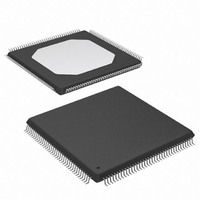
XC3S250E-4TQG144C Xilinx Inc, XC3S250E-4TQG144C Datasheet - Page 53

XC3S250E-4TQG144C
Manufacturer Part Number
XC3S250E-4TQG144C
Description
IC SPARTAN-3E FPGA 250K 144TQFP
Manufacturer
Xilinx Inc
Series
Spartan™-3Er
Datasheet
1.XC3S100E-4VQG100C.pdf
(233 pages)
Specifications of XC3S250E-4TQG144C
Number Of Logic Elements/cells
5508
Number Of Labs/clbs
612
Total Ram Bits
221184
Number Of I /o
108
Number Of Gates
250000
Voltage - Supply
1.14 V ~ 1.26 V
Mounting Type
Surface Mount
Operating Temperature
0°C ~ 85°C
Package / Case
144-LQFP
For Use With
813-1009 - MODULE USB-TO-FPGA TOOL W/MANUAL
Lead Free Status / RoHS Status
Lead free / RoHS Compliant
Other names
122-1524
Available stocks
Company
Part Number
Manufacturer
Quantity
Price
Company:
Part Number:
XC3S250E-4TQG144C
Manufacturer:
XILINX
Quantity:
2 000
Company:
Part Number:
XC3S250E-4TQG144C
Manufacturer:
XILINX
Quantity:
2 400
Company:
Part Number:
XC3S250E-4TQG144C
Manufacturer:
Xilinx Inc
Quantity:
10 000
Part Number:
XC3S250E-4TQG144C
Manufacturer:
XILINX/赛灵思
Quantity:
20 000
Part Number:
XC3S250E-4TQG144CS1
Manufacturer:
XILINX/赛灵思
Quantity:
20 000
Every FPGA input provides a possible DCM clock input, but
the path is not temperature and voltage compensated like
the GCLKs. Alternatively, clock signals within the FPGA
optionally provide a DCM clock input via a Global Clock
Multiplexer Buffer (BUFGMUX). The global clock net con-
nects directly to the CLKIN input. The internal and external
connections are shown in
respectively.
DLL Clock Output and Feedback Connections
As many as four of the nine DCM clock outputs can simulta-
neously drive four of the BUFGMUX buffers on the same die
edge. All DCM clock outputs can simultaneously drive gen-
eral routing resources, including interconnect leading to
OBUF buffers.
The feedback loop is essential for DLL operation. Either the
CLK0 or CLK2X outputs feed back to the CLKFB input via a
BUFGMUX global buffer to eliminate the clock distribution
delay. The specific BUFGMUX buffer used to feed back the
CLK0 or CLK2X signal is ideally one of the BUFGMUX buff-
ers associated with a specific DCM, as shown in
Table
The feedback path also phase-aligns the other seven DLL
outputs: CLK0, CLK90, CLK180, CLK270, CLKDV, CLK2X,
or CLK2X180. The CLK_FEEDBACK attribute value must
agree with the physical feedback connection. Use “1X” for
DS312-2 (v3.8) August 26, 2009
Product Specification
31, and
BUFG
R
IBUFG
IBUFG
Table
(c) Off-Chip with CLK0 Feedback
(a) On-Chip with CLK0 Feedback
Figure 42: Input Clock, Output Clock, and Feedback Connections for the DLL
32.
CLKIN
CLKFB
CLKIN
CLKFB
DCM
DCM
FPGA
CLK2X180
CLK2X180
FPGA
CLK0
CLK0
CLK180
CLK270
CLK180
CLK270
CLKDV
CLKDV
CLK2X
CLK2X
CLK90
CLK90
Figure 42a
CLK0
CLK0
BUFGMUX
BUFGMUX
OBUF
OBUF
and
Net Delay
Clock
Net Delay
Figure
Clock
Table
www.xilinx.com
42c,
30,
CLK0 feedback and “2X” for CLK2X feedback. If the DFS
unit is used stand-alone, without the DLL, then no feedback
is required and set the CLK_FEEDBACK attribute to
“NONE”.
Two basic cases determine how to connect the DLL clock
outputs and feedback connections: on-chip synchronization
and off-chip synchronization, which are illustrated in
Figure 42a
In the on-chip synchronization case in
Figure
output clock signals through general routing resources to
the FPGA’s internal registers. Either a Global Clock Buffer
(BUFG) or a BUFGMUX affords access to the global clock
network. As shown in
ated by routing CLK0 (or CLK2X) in
clock net, which in turn drives the CLKFB input.
In the off-chip synchronization case in
Figure
output clock signals exit the FPGA using output buffers
(OBUF) to drive an external clock network plus registers on
the board. As shown in
formed by feeding CLK0 (or CLK2X) in
the FPGA, then to the DCM’s CLKFB input via a Global
Buffer Input, specified in
BUFG
IBUFG
IBUFG
42b, it is possible to connect any of the DLL’s seven
42d, CLK0 (or CLK2X) plus any of the DLL’s other
(d) Off-Chip with CLK2X Feedback
(b) On-Chip with CLK2X Feedback
through
CLKIN
CLKFB
CLKIN
CLKFB
DCM
DCM
FPGA
Figure
CLK2X180
CLK2X180
CLK2X
CLK2X
FPGA
Figure
CLK180
CLK270
CLK180
CLK270
CLKDV
CLKDV
CLK90
CLK90
CLK2X
CLK2X
CLK0
CLK0
Table
Figure
42d.
42a, the feedback loop is cre-
30.
BUFGMUX
BUFGMUX
OBUF
OBUF
42c, the feedback loop is
Functional Description
Figure 42b
Figure 42d
Net Delay
Clock
Net Delay
DS099-2_09_082104
Clock
Figure 42a
Figure 42c
to a global
back into
and
and
53


