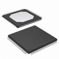
XC3S250E-4TQG144C Xilinx Inc, XC3S250E-4TQG144C Datasheet - Page 54

XC3S250E-4TQG144C
Manufacturer Part Number
XC3S250E-4TQG144C
Description
IC SPARTAN-3E FPGA 250K 144TQFP
Manufacturer
Xilinx Inc
Series
Spartan™-3Er
Datasheet
1.XC3S100E-4VQG100C.pdf
(233 pages)
Specifications of XC3S250E-4TQG144C
Number Of Logic Elements/cells
5508
Number Of Labs/clbs
612
Total Ram Bits
221184
Number Of I /o
108
Number Of Gates
250000
Voltage - Supply
1.14 V ~ 1.26 V
Mounting Type
Surface Mount
Operating Temperature
0°C ~ 85°C
Package / Case
144-LQFP
For Use With
813-1009 - MODULE USB-TO-FPGA TOOL W/MANUAL
Lead Free Status / RoHS Status
Lead free / RoHS Compliant
Other names
122-1524
Available stocks
Company
Part Number
Manufacturer
Quantity
Price
Company:
Part Number:
XC3S250E-4TQG144C
Manufacturer:
XILINX
Quantity:
2 000
Company:
Part Number:
XC3S250E-4TQG144C
Manufacturer:
XILINX
Quantity:
2 400
Company:
Part Number:
XC3S250E-4TQG144C
Manufacturer:
Xilinx Inc
Quantity:
10 000
Part Number:
XC3S250E-4TQG144C
Manufacturer:
XILINX/赛灵思
Quantity:
20 000
Part Number:
XC3S250E-4TQG144CS1
Manufacturer:
XILINX/赛灵思
Quantity:
20 000
Functional Description
Accommodating Input Frequencies Beyond Spec-
ified Maximums
If the CLKIN input frequency exceeds the maximum permit-
ted, divide it down to an acceptable value using the
CLKIN_DIVIDE_BY_2 attribute. When this attribute is set to
“TRUE”, the CLKIN frequency is divided by a factor of two
as it enters the DCM. In addition, the CLKIN_DIVIDE_BY_2
option produces a 50% duty-cycle on the input clock,
although at half the CLKIN frequency.
Quadrant and Half-Period Phase Shift Outputs
In addition to CLK0 for zero-phase alignment to the CLKIN
signal, the DLL also provides the CLK90, CLK180, and
CLK270 outputs for 90°, 180°, and 270° phase-shifted sig-
nals, respectively. These signals are described in
page 49
control in finer increments than 90°, see
(PS).
Basic Frequency Synthesis Outputs
The DLL component provides basic options for frequency
multiplication and division in addition to the more flexible
synthesis capability of the DFS component, described in a
later section. These operations result in output clock signals
with frequencies that are either a fraction (for division) or a
multiple (for multiplication) of the incoming clock frequency.
54
Phase:
Input Signal (40%/60% Duty Cycle)
Output Signal - Duty Cycle Corrected
CLK2X180
Figure 43: Characteristics of the DLL Clock Outputs
CLK180
CLK270
CLKDV
CLK2X
CLK90
CLKIN
CLK0
and their relative timing is shown in
0
o
90
o
180
t
o
270
o
0
o
90
o
180
Phase Shifter
Figure
o
270
DS099-2_10_101105
Table 28,
o
43. For
www.xilinx.com
0
o
The CLK2X output produces an in-phase signal that is twice
the frequency of CLKIN. The CLK2X180 output also dou-
bles the frequency, but is 180° out-of-phase with respect to
CLKIN. The CLKDIV output generates a clock frequency
that is a predetermined fraction of the CLKIN frequency.
The CLKDV_DIVIDE attribute determines the factor used to
divide the CLKIN frequency. The attribute can be set to var-
ious values as described in
synthesis outputs are described in
Duty Cycle Correction of DLL Clock Outputs
The DLL output signals exhibit a 50% duty cycle, even if the
incoming CLKIN signal has a different duty cycle. Fifty-per-
cent duty cycle means that the High and Low times of each
clock cycle are equal.
DLL Performance Differences Between Steppings
As indicated in
(Module 3), the Stepping 1 revision silicon supports higher
maximum input and output frequencies. Stepping 1 devices
are backwards compatible with Stepping 0 devices.
Digital Frequency Synthesizer (DFS)
The DFS unit generates clock signals where the output fre-
quency is a product of the CLKIN input clock frequency and
a ratio of two user-specified integers. The two dedicated
outputs from the DFS unit, CLKFX and CLKFX180, are
defined in
Table 33: DFS Signals
The signal at the CLKFX180 output is essentially an inver-
sion of the CLKFX signal. These two outputs always exhibit
a 50% duty cycle, even when the CLKIN signal does not.
The DFS clock outputs are active coincident with the seven
DLL outputs and their output phase is controlled by the
Phase Shifter unit (PS).
The output frequency (f
incoming clock frequency (f
attributes, as follows.
The CLKFX_MULTIPLY attribute is an integer ranging from
2 to 32, inclusive, and forms the numerator in
CLKFX
CLKFX180
Signal
f
CLKFX
Table
Output
Output
Direction
=
33.
Digital Clock Manager (DCM) Timing
f
CLKIN
CLKFX
•
⎛
⎝
CLKFX_MULTIPLY
--------------------------------------------------- -
Multiplies the CLKIN frequency
by the attribute-value ratio
(CLKFX_MULTIPLY/
CLKFX_DIVIDE) to generate a
clock signal with a new target
frequency.
Generates a clock signal with
the same frequency as CLKFX,
but shifted 180° out-of-phase.
CLKFX_DIVIDE
Table
) of the DFS is a function of the
DS312-2 (v3.8) August 26, 2009
CLKIN
29. The basic frequency
Table
Description
) and two integer
Product Specification
28.
⎞
⎠
Equation
Eq. 1
1.
R


