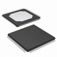
XC3S250E-4TQG144C Xilinx Inc, XC3S250E-4TQG144C Datasheet - Page 62

XC3S250E-4TQG144C
Manufacturer Part Number
XC3S250E-4TQG144C
Description
IC SPARTAN-3E FPGA 250K 144TQFP
Manufacturer
Xilinx Inc
Series
Spartan™-3Er
Datasheet
1.XC3S100E-4VQG100C.pdf
(233 pages)
Specifications of XC3S250E-4TQG144C
Number Of Logic Elements/cells
5508
Number Of Labs/clbs
612
Total Ram Bits
221184
Number Of I /o
108
Number Of Gates
250000
Voltage - Supply
1.14 V ~ 1.26 V
Mounting Type
Surface Mount
Operating Temperature
0°C ~ 85°C
Package / Case
144-LQFP
For Use With
813-1009 - MODULE USB-TO-FPGA TOOL W/MANUAL
Lead Free Status / RoHS Status
Lead free / RoHS Compliant
Other names
122-1524
Available stocks
Company
Part Number
Manufacturer
Quantity
Price
Company:
Part Number:
XC3S250E-4TQG144C
Manufacturer:
XILINX
Quantity:
2 000
Company:
Part Number:
XC3S250E-4TQG144C
Manufacturer:
XILINX
Quantity:
2 400
Company:
Part Number:
XC3S250E-4TQG144C
Manufacturer:
Xilinx Inc
Quantity:
10 000
Part Number:
XC3S250E-4TQG144C
Manufacturer:
XILINX/赛灵思
Quantity:
20 000
Part Number:
XC3S250E-4TQG144CS1
Manufacturer:
XILINX/赛灵思
Quantity:
20 000
Functional Description
Quadrant Clock Routing
The clock routing within the FPGA is quadrant-based, as
shown in
total clock signals, labeled ‘A’ through ‘H’ in
Figure
inates either from a global BUFGMUX element along the
top and bottom edges or from a BUFGMUX element along
the associated edge, as shown in
feed the synchronous resource elements (CLBs, IOBs,
block RAM, multipliers, and DCMs) within the quadrant.
The four quadrants of the device are:
•
•
•
•
Note that the quadrant clock notation (TR, BR, BL, TL) is
separate from that used for similar IOB placement con-
straints.
To estimate the quadrant location for a particular I/O, see
the footprint diagrams in
For exact quadrant locations, use the floorplanning tool. In
the QFP packages (TQ144 and PQ208) the quadrant bor-
ders fall in the middle of each side of the package, at a GND
pin. The clock inputs fall on the quadrant boundaries, as
indicated in
62
Top Right (TR)
Bottom Right (BR)
Bottom Left (BL)
Top Left (TL)
47. The clock source for an individual clock line orig-
Figure
Table
45. Each clock quadrant supports eight
42.
*(XC3S1200E and
RHCLK input
Double Line
XC3S1600E only)
DCM output*
LHCLK or
Pinout Descriptions
Figure 46: Clock Switch Matrix to BUFGMUX Pair Connectivity
CLK Switch
Figure
Left-/Right-Half BUFGMUX
Matrix
47. The clock lines
Table 41
(Module 4).
S
S
I0
I1
I0
I1
www.xilinx.com
0
1
0
1
and
BUFGMUX
O
O
2nd DCM output
1st DCM output
2nd GCLK pin
1st GCLK pin
Double Line
Table 42: QFP Package Clock Quadrant Locations
In a few cases, a dedicated input is physically in one quad-
rant of the device but connects to a different clock quadrant:
•
•
•
•
FT256, H16 is in clock quadrant BR
FG320, K2 is in clock quadrant BL
FG400, L8 is in clock quadrant TL and the I/O at N11 is
in clock quadrant BL
FG484, M2 is in clock quadrant TL and L15 is in clock
quadrant BR
GCLK[15:12]
RHCLK[3:0]
RHCLK[7:4]
GCLK[11:8]
Clock Pins
LHCLK[3:0]
LHCLK[7:4]
GCLK[3:0]
GCLK[7:4]
Top/Bottom (Global) BUFGMUX
CLK Switch
Matrix
DS312-2 (v3.8) August 26, 2009
S
S
I0
I1
I0
I1
0
1
0
1
DS312-2_16_110706
BUFGMUX
O
O
Product Specification
Quadrant
BR
BR
TR
TR
TL
BL
TL
BL
R


