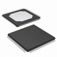
XC3S250E-4TQG144C Xilinx Inc, XC3S250E-4TQG144C Datasheet - Page 79

XC3S250E-4TQG144C
Manufacturer Part Number
XC3S250E-4TQG144C
Description
IC SPARTAN-3E FPGA 250K 144TQFP
Manufacturer
Xilinx Inc
Series
Spartan™-3Er
Datasheet
1.XC3S100E-4VQG100C.pdf
(233 pages)
Specifications of XC3S250E-4TQG144C
Number Of Logic Elements/cells
5508
Number Of Labs/clbs
612
Total Ram Bits
221184
Number Of I /o
108
Number Of Gates
250000
Voltage - Supply
1.14 V ~ 1.26 V
Mounting Type
Surface Mount
Operating Temperature
0°C ~ 85°C
Package / Case
144-LQFP
For Use With
813-1009 - MODULE USB-TO-FPGA TOOL W/MANUAL
Lead Free Status / RoHS Status
Lead free / RoHS Compliant
Other names
122-1524
Available stocks
Company
Part Number
Manufacturer
Quantity
Price
Company:
Part Number:
XC3S250E-4TQG144C
Manufacturer:
XILINX
Quantity:
2 000
Company:
Part Number:
XC3S250E-4TQG144C
Manufacturer:
XILINX
Quantity:
2 400
Company:
Part Number:
XC3S250E-4TQG144C
Manufacturer:
Xilinx Inc
Quantity:
10 000
Part Number:
XC3S250E-4TQG144C
Manufacturer:
XILINX/赛灵思
Quantity:
20 000
Part Number:
XC3S250E-4TQG144CS1
Manufacturer:
XILINX/赛灵思
Quantity:
20 000
PROM and the FPGA’s SPI configuration interface. Each
SPI Flash PROM vendor uses slightly different signal nam-
ing. The SPI Flash PROM’s write protect and hold controls
Table 54: Example SPI Flash PROM Connections and Pin Naming
The mode select pins, M[2:0], and the variant select pins,
VS[2:0] are sampled when the FPGA’s INIT_B output goes
High and must be at defined logic levels during this time.
After configuration, when the FPGA’s DONE output goes
High, these pins are all available as full-featured user-I/O
pins.
enable pull-up resistors on all user-I/O pins or High to dis-
DS312-2 (v3.8) August 26, 2009
Product Specification
W
DATA_IN
DATA_OUT
SELECT
CLOCK
WR_PROTECT
HOLD
(see
RESET
(see
RDY/BUSY
(see
P
SPI Flash Pin
Table 54
Similarly, the FPGA’s HSWAP pin must be Low to
Figure
Figure
Figure
W
R
shows the connections between the SPI Flash
53)
54)
54)
MOSI
DIN
CSO_B
CCLK
Not required for FPGA configuration. Must be
High to program SPI Flash. Optional
connection to FPGA user I/O after
configuration.
Not required for FPGA configuration but must
be High during configuration. Optional
connection to FPGA user I/O after
configuration. Not applicable to Atmel
DataFlash.
Only applicable to Atmel DataFlash. Not
required for FPGA configuration but must be
High during configuration. Optional
connection to FPGA user I/O after
configuration. Do not connect to FPGA’s
PROG_B as this will prevent direct
programming of the DataFlash.
Only applicable to Atmel DataFlash and only
available on certain packages. Not required
for FPGA configuration. Output from
DataFlash PROM. Optional connection to
FPGA user I/O after configuration.
FPGA Connection
www.xilinx.com
are not used by the FPGA during configuration. However,
the HOLD pin must be High during the configuration pro-
cess. The PROM’s write protect input must be High in order
to write or program the Flash memory.
able the pull-up resistors. The HSWAP control must remain
at a constant logic level throughout FPGA configuration.
After configuration, when the FPGA’s DONE output goes
High, the HSWAP pin is available as full-featured user-I/O
pin and is powered by the VCCO_0 supply.
In a single-FPGA application, the FPGA’s DOUT pin is not
used but is actively driving during the configuration process.
STMicro
HOLD
N/A
N/A
W
Q
D
S
C
NexFlash
HOLD
CLK
WP
N/A
N/A
DO
CS
DI
Technology
Storage
Silicon
HOLD#
WP#
SCK
CE#
N/A
N/A
SO
Functional Description
SI
RDY/BUSY
DataFlash
RESET
Atmel
SCK
N/A
WP
SO
CS
SI
79


