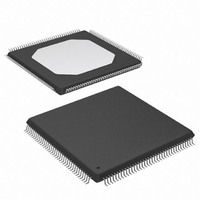
XC3S250E-4TQG144C Xilinx Inc, XC3S250E-4TQG144C Datasheet - Page 81

XC3S250E-4TQG144C
Manufacturer Part Number
XC3S250E-4TQG144C
Description
IC SPARTAN-3E FPGA 250K 144TQFP
Manufacturer
Xilinx Inc
Series
Spartan™-3Er
Datasheet
1.XC3S100E-4VQG100C.pdf
(233 pages)
Specifications of XC3S250E-4TQG144C
Number Of Logic Elements/cells
5508
Number Of Labs/clbs
612
Total Ram Bits
221184
Number Of I /o
108
Number Of Gates
250000
Voltage - Supply
1.14 V ~ 1.26 V
Mounting Type
Surface Mount
Operating Temperature
0°C ~ 85°C
Package / Case
144-LQFP
For Use With
813-1009 - MODULE USB-TO-FPGA TOOL W/MANUAL
Lead Free Status / RoHS Status
Lead free / RoHS Compliant
Other names
122-1524
Available stocks
Company
Part Number
Manufacturer
Quantity
Price
Company:
Part Number:
XC3S250E-4TQG144C
Manufacturer:
XILINX
Quantity:
2 000
Company:
Part Number:
XC3S250E-4TQG144C
Manufacturer:
XILINX
Quantity:
2 400
Company:
Part Number:
XC3S250E-4TQG144C
Manufacturer:
Xilinx Inc
Quantity:
10 000
Part Number:
XC3S250E-4TQG144C
Manufacturer:
XILINX/赛灵思
Quantity:
20 000
Part Number:
XC3S250E-4TQG144CS1
Manufacturer:
XILINX/赛灵思
Quantity:
20 000
Table 55: Serial Peripheral Interface (SPI) Connections (Continued)
Voltage Compatibility
Available SPI Flash PROMs use a single 3.3V supply volt-
age. All of the FPGA’s SPI Flash interface signals are within
I/O Bank 2. Consequently, the FPGA’s VCCO_2 supply volt-
age must also be 3.3V to match the SPI Flash PROM.
Power-On Precautions if 3.3V Supply is Last in
Sequence
Spartan-3E FPGAs have a built-in power-on reset (POR)
circuit, as shown in
Table 56: Example Minimum Power-On to Select Times for Various SPI Flash PROMs
In many systems, the 3.3V supply feeding the FPGA's
VCCO_2 input is valid before the FPGA's other V
V
DS312-2 (v3.8) August 26, 2009
Product Specification
DONE
PROG_B
STMicroelectronics
Spansion
NexFlash
Macronix
Silicon Storage Technology
Programmable
Microelectronics Corporation
Atmel Corporation
CCAUX
Pin Name
supplies, and consequently, there is no issue. How-
Vendor
R
bidirectional
Open-drain
Direction
FPGA
Input
I/O
Figure
66. The FPGA waits for its three
FPGA Configuration Done. Low during
configuration. Goes High when FPGA
successfully completes configuration.
Requires external 330 Ω pull-up resistor
to 2.5V.
Program FPGA. Active Low. When
asserted Low for 500 ns or longer, forces
the FPGA to restart its configuration
process by clearing configuration
memory and resetting the DONE and
INIT_B pins once PROG_B returns
High. Recommend external 4.7 kΩ
pull-up resistor to 2.5V. Internal pull-up
value may be weaker (see
driving externally with a 3.3V output, use
an open-drain or open-collector driver or
use a current limiting series resistor.
SPI Flash PROM
Part Number
AT45DBxxxD
AT45DBxxxB
SST25LFxx
Pm25LVxxx
S25FLxxxA
MX25Lxxxx
M25Pxx
Description
NX25xx
CCINT
Table
www.xilinx.com
and
78). If
Data Sheet Minimum Time from V
power supplies
(VCCO_2)
before beginning the configuration process.
The SPI Flash PROM is powered by the same voltage sup-
ply feeding the FPGA's VCCO_2 voltage input, typically
3.3V. SPI Flash PROMs specify that they cannot be
accessed until their V
sheet voltage, followed by an additional delay. For some
devices, this additional delay is as little as 10 µs as shown in
Table
ever, if the 3.3V supply feeding the FPGA's VCCO_2 supply
is last in the sequence, a potential race occurs between the
FPGA and the SPI Flash PROM, as shown in
T
Symbol
PU-READ
Low indicates that the FPGA is
not yet configured.
Must be High to allow
configuration to start.
t
T
T
T
t
VCSL
t
VSL
VCS
VSL
PU
VSL
56. For other vendors, this delay is as much as 20 ms.
During Configuration
—
to reach their respective power-on thresholds
—
V
CCINT
CC
Value
supply reaches its minimum data
, V
10
10
10
10
10
50
30
20
CCAUX
CC
Pulled High via external
pull-up. When High,
indicates that the FPGA
successfully configured.
Drive PROG_B Low and
release to reprogram
FPGA. Hold PROG_B to
force FPGA I/O pins into
Hi-Z, allowing direct
programming access to SPI
Flash PROM pins.
Functional Description
, and V
min to Select = Low
After Configuration
CCO
Figure
to I/O Bank 2
Units
ms
ms
μs
μs
μs
μs
μs
μs
55.
81


