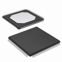
XC3S250E-4TQG144C Xilinx Inc, XC3S250E-4TQG144C Datasheet - Page 83

XC3S250E-4TQG144C
Manufacturer Part Number
XC3S250E-4TQG144C
Description
IC SPARTAN-3E FPGA 250K 144TQFP
Manufacturer
Xilinx Inc
Series
Spartan™-3Er
Datasheet
1.XC3S100E-4VQG100C.pdf
(233 pages)
Specifications of XC3S250E-4TQG144C
Number Of Logic Elements/cells
5508
Number Of Labs/clbs
612
Total Ram Bits
221184
Number Of I /o
108
Number Of Gates
250000
Voltage - Supply
1.14 V ~ 1.26 V
Mounting Type
Surface Mount
Operating Temperature
0°C ~ 85°C
Package / Case
144-LQFP
For Use With
813-1009 - MODULE USB-TO-FPGA TOOL W/MANUAL
Lead Free Status / RoHS Status
Lead free / RoHS Compliant
Other names
122-1524
Available stocks
Company
Part Number
Manufacturer
Quantity
Price
Company:
Part Number:
XC3S250E-4TQG144C
Manufacturer:
XILINX
Quantity:
2 000
Company:
Part Number:
XC3S250E-4TQG144C
Manufacturer:
XILINX
Quantity:
2 400
Company:
Part Number:
XC3S250E-4TQG144C
Manufacturer:
Xilinx Inc
Quantity:
10 000
Part Number:
XC3S250E-4TQG144C
Manufacturer:
XILINX/赛灵思
Quantity:
20 000
Part Number:
XC3S250E-4TQG144CS1
Manufacturer:
XILINX/赛灵思
Quantity:
20 000
If not using the SPI Flash PROM after configuration, drive
CSO_B High to disable the PROM. The MOSI, DIN, and
CCLK pins are then available to the FPGA application.
Because all the interface pins are user I/O after configura-
tion, the FPGA application can continue to use the SPI
Flash interface pins to communicate with the SPI Flash
PROM, as shown in
dom-accessible, byte-addressable, read/write, non-volatile
storage to the FPGA application.
SPI Flash PROMs are available in densities ranging from
1 Mbit up to 128 Mbits. However, a single Spartan-3E FPGA
requires less than 6 Mbits. If desired, use a larger SPI Flash
PROM to contain additional non-volatile application data,
such as MicroBlaze processor code, or other user data such
as serial numbers and Ethernet MAC IDs. In the example
shown in
PROM. Then using FPGA logic after configuration, the
FPGA copies MicroBlaze code from SPI Flash into external
DDR SDRAM for code execution. Similarly, the FPGA appli-
cation can store non-volatile application data within the SPI
Flash PROM.
The FPGA configuration data is stored starting at location 0.
Store any additional data beginning in the next available SPI
Flash PROM sector or page. Do not mix configuration data
and user data in the same sector or page.
DS312-2 (v3.8) August 26, 2009
Product Specification
Figure
R
56, the FPGA configures from SPI Flash
Figure
56. SPI Flash PROMs offer ran-
Spartan-3E FPGA
Figure 56: Using the SPI Flash Interface After Configuration
FPGA-based
SPI Master
User I/O
CSO_B
CCLK
MOSI
DIN
To other SPI slave peripherals
www.xilinx.com
Similarly, the SPI bus can be expanded to additional SPI
peripherals. Because SPI is a common industry-standard
interface, various SPI-based peripherals are available, such
as analog-to-digital (A/D) converters, digital-to-analog (D/A)
converters, CAN controllers, and temperature sensors.
However, if sufficient I/O pins are available in the applica-
tion, Xilinx recommends creating a separate SPI bus to con-
trol peripherals. Creating a second port reduces the loading
on the CCLK and DIN pins, which are crucial for configura-
tion.
The MOSI, DIN, and CCLK pins are common to all SPI
peripherals. Connect the select input on each additional SPI
peripheral to one of the FPGA user I/O pins. If HSWAP = 0
during configuration, the FPGA holds the select line High. If
HSWAP = 1, connect the select line to +3.3V via an external
4.7 kΩ pull-up resistor to avoid spurious read or write oper-
ations. After configuration, drive the select line Low to select
the desired SPI peripheral.
During the configuration process, CCLK is controlled by the
FPGA and limited to the frequencies generated by the
FPGA. After configuration, the FPGA application can use
other clock signals to drive the CCLK pin and can further
optimize SPI-based communication.
Refer to the individual SPI peripheral data sheet for specific
interface and communication protocol requirements.
+3.3V
SPI Serial Flash PROM
SPI Peripherals
DATA_IN
DATA_OUT
CLOCK
DATA_IN
DATA_OUT
CLOCK
SELECT
SELECT
- A/D Converter
- D/A Converter
- CAN Controller
- Displays
- Temperature Sensor
- ASSP
Configuration
MicroBlaze
User Data
FPGA
Code
Functional Description
DS312-2_47_082009
FFFFF
0
83


