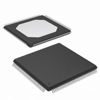
XC3S250E-4TQG144C Xilinx Inc, XC3S250E-4TQG144C Datasheet - Page 92

XC3S250E-4TQG144C
Manufacturer Part Number
XC3S250E-4TQG144C
Description
IC SPARTAN-3E FPGA 250K 144TQFP
Manufacturer
Xilinx Inc
Series
Spartan™-3Er
Datasheet
1.XC3S100E-4VQG100C.pdf
(233 pages)
Specifications of XC3S250E-4TQG144C
Number Of Logic Elements/cells
5508
Number Of Labs/clbs
612
Total Ram Bits
221184
Number Of I /o
108
Number Of Gates
250000
Voltage - Supply
1.14 V ~ 1.26 V
Mounting Type
Surface Mount
Operating Temperature
0°C ~ 85°C
Package / Case
144-LQFP
For Use With
813-1009 - MODULE USB-TO-FPGA TOOL W/MANUAL
Lead Free Status / RoHS Status
Lead free / RoHS Compliant
Other names
122-1524
Available stocks
Company
Part Number
Manufacturer
Quantity
Price
Company:
Part Number:
XC3S250E-4TQG144C
Manufacturer:
XILINX
Quantity:
2 000
Company:
Part Number:
XC3S250E-4TQG144C
Manufacturer:
XILINX
Quantity:
2 400
Company:
Part Number:
XC3S250E-4TQG144C
Manufacturer:
Xilinx Inc
Quantity:
10 000
Part Number:
XC3S250E-4TQG144C
Manufacturer:
XILINX/赛灵思
Quantity:
20 000
Part Number:
XC3S250E-4TQG144CS1
Manufacturer:
XILINX/赛灵思
Quantity:
20 000
Functional Description
Table 63: FPGA Connections to Flash PROM with IO15/A-1 Pin (Continued)
Some x8/x16 Flash PROMs have a long setup time require-
ment on the BYTE# signal. For the FPGA to configure cor-
rectly, the PROM must be in x8 mode with BYTE# = 0 at
power-on or when the FPGA’s PROG_B pin is pulsed Low.
If required, extend the BYTE# setup time for a 3.3V PROM
using an external 680 Ω pull-down resistor on the FPGA’s
LDC2 pin or by delaying assertion of the CSI_B select input
to the FPGA.
Daisy-Chaining
If the application requires multiple FPGAs with different con-
figurations, then configure the FPGAs using a daisy chain,
as shown in
<0:1:1>) for the FPGA connected to the parallel NOR Flash
PROM and Slave Parallel mode (M[2:0] = <1:1:0>) for all
downstream FPGAs in the daisy-chain. If there are more
than two FPGAs in the chain, then last FPGA in the chain
can be from any Xilinx FPGA family. However, all intermedi-
ate FPGAs located in the chain between the first and last
FPGAs must from either the Spartan-3E or Virtex®-5 FPGA
families.
After the master FPGA—the FPGA on the left in the dia-
gram—finishes loading its configuration data from the paral-
lel Flash PROM, the master device continues generating
addresses to the Flash PROM and asserts its CSO_B out-
put Low, enabling the next FPGA in the daisy-chain. The
next FPGA then receives parallel configuration data from
the Flash PROM. The master FPGA’s CCLK output syn-
chronizes data capture.
If HSWAP = 1, an external 4.7kΩ pull-up resistor must be
added on the CSO_B pin. If HSWAP = 0, no external pull-up
is necessary.
Design Note
BPI mode daisy chain software support is available starting
in ISE 8.2i.
http://www.xilinx.com/support/answers/23061.htm
Also, in a multi-FPGA daisy-chain configuration of more
than two devices, all intermediate FPGAs between the first
92
A[23:1]
A0
D[7:0]
User I/O
FPGA Pin
Figure
A[n:0]
IO15/A-1
IO[7:0]
Upper data lines IO[14:8] not
required unless used as x16 Flash
interface after configuration
Connection to Flash PROM with
59. Use BPI mode (M[2:0] = <0:1:0> or
IO15/A-1 Pin
x8 Flash PROM Interface After
A[n:0]
IO15/A-1 is the least-significant
address input
IO[7:0]
Upper data lines IO[14:8] not
required
www.xilinx.com
FPGA Configuration
and last devices must be Spartan-3E or Virtex-5 FPGAs.
The last FPGA in the chain can be from any Xilinx FPGA
family.
BPI Mode Interaction with Right and Bottom Edge
Global Clock Inputs
Some of the BPI mode configuration pins are shared with
global clock inputs along the right and bottom edges of the
device (Bank 1 and Bank 2, respectively). These pins are
not easily reclaimable for clock inputs after configuration,
especially if the FPGA application access the parallel NOR
Flash after configuration.
pins.
Table 64: Shared BPI Configuration Mode and Global
Buffer Input Pins
Device
Bottom
Edge
Right
Global Buffer
Input Pin
GCLK12
GCLK13
GCLK14
GCLK15
RHCLK0
RHCLK1
RHCLK2
RHCLK3
RHCLK4
RHCLK5
RHCLK6
RHCLK7
GCLK0
GCLK2
GCLK3
A[n:0]
IO15/A-1 is the most-significant
data line, IO15
IO[7:0]
IO[14:8]
x16 Flash PROM Interface After
Table 64
DS312-2 (v3.8) August 26, 2009
FPGA Configuration
summarizes the shared
Configuration Pin
Product Specification
BPI Mode
RDWR_B
A10
D2
D1
D7
D6
D4
D3
A9
A8
A7
A6
A5
A4
A3
R


