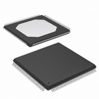
XC3S250E-4TQG144C Xilinx Inc, XC3S250E-4TQG144C Datasheet - Page 93

XC3S250E-4TQG144C
Manufacturer Part Number
XC3S250E-4TQG144C
Description
IC SPARTAN-3E FPGA 250K 144TQFP
Manufacturer
Xilinx Inc
Series
Spartan™-3Er
Datasheet
1.XC3S100E-4VQG100C.pdf
(233 pages)
Specifications of XC3S250E-4TQG144C
Number Of Logic Elements/cells
5508
Number Of Labs/clbs
612
Total Ram Bits
221184
Number Of I /o
108
Number Of Gates
250000
Voltage - Supply
1.14 V ~ 1.26 V
Mounting Type
Surface Mount
Operating Temperature
0°C ~ 85°C
Package / Case
144-LQFP
For Use With
813-1009 - MODULE USB-TO-FPGA TOOL W/MANUAL
Lead Free Status / RoHS Status
Lead free / RoHS Compliant
Other names
122-1524
Available stocks
Company
Part Number
Manufacturer
Quantity
Price
Company:
Part Number:
XC3S250E-4TQG144C
Manufacturer:
XILINX
Quantity:
2 000
Company:
Part Number:
XC3S250E-4TQG144C
Manufacturer:
XILINX
Quantity:
2 400
Company:
Part Number:
XC3S250E-4TQG144C
Manufacturer:
Xilinx Inc
Quantity:
10 000
Part Number:
XC3S250E-4TQG144C
Manufacturer:
XILINX/赛灵思
Quantity:
20 000
Part Number:
XC3S250E-4TQG144CS1
Manufacturer:
XILINX/赛灵思
Quantity:
20 000
Stepping 0 Limitations when Reprogramming via
JTAG if FPGA Set for BPI Configuration
The FPGA can always be reprogrammed via the JTAG port,
regardless of the mode pin (M[2:0]) settings. However,
Stepping 0 devices have a minor limitation. If a Stepping 0
FPGA is set to configure in BPI mode and the FPGA is
attached to a parallel memory containing a valid FPGA con-
In-System Programming Support
usually preprogrammed before it is mounted on the printed
circuit board. In-system programming support is available
from third-party boundary-scan tool vendors and from some
third-party PROM programmers using a socket adapter with
attached wires. To gain access to the parallel Flash signals,
drive the FPGA’s PROG_B input Low with an open-drain
driver. This action places all FPGA I/O pins, including those
attached to the parallel Flash, in high-impedance (Hi-Z). If
the HSWAP input is Low, the I/Os have pull-up resistors to
the V
programming hardware then has direct access to the paral-
DS312-2 (v3.8) August 26, 2009
Product Specification
I
Recommend
open-drain
PROG_B
In a production application, the parallel Flash PROM is
driver
CCO
TMS
TCK
TDO
TDI
JTAG
2.5V
input on their respective I/O bank. The external
R
Not available
in VQ100
package
BPI Mode
‘0’
‘1’
A
‘0’
‘0’
P
HSWAP
M2
M1
M0
CSI_B
RDWR_B
TDI
TMS
TCK
PROG_B
Spartan-3E
FPGA
VCCINT
+1.2V
GND
VCCAUX
VCCO_0
VCCO_1
VCCO_2
A[23:17]
Figure 59: Daisy-Chaining from BPI Flash Mode
CSO_B
A[16:0]
INIT_B
DONE
BUSY
D[7:0]
CCLK
LDC0
LDC1
LDC2
HDC
TDO
VCCO_0
+2.5V
V
V
www.xilinx.com
I
+2.5V
CE#
OE#
WE#
BYTE#
DQ[15:7]
DQ[7:0]
A[n:0]
VCC
GND
figuration file, then subsequent reconfigurations using the
JTAG port will fail. Potential workarounds include setting the
mode pins for JTAG configuration (M[2:0] = <1:0:1>) or off-
setting the initial memory location in Flash by 0x2000.
Stepping 1 devices fully support JTAG configuration even
when the FPGA mode pins are set for BPI mode.
lel Flash pins. The programming access points are high-
lighted in the gray boxes in
The FPGA itself can also be used as a parallel Flash PROM
programmer during development and test phases. Initially,
an FPGA-based programmer is downloaded into the FPGA
via JTAG. Then the FPGA performs the Flash PROM pro-
gramming algorithms and receives programming data from
the host via the FPGA’s JTAG interface. See the Embedded
System Tools Reference Manual.
Dynamically Loading Multiple Configuration
Images Using MultiBoot Option
For additional information, refer to the “Reconfiguration and
MultiBoot” chapter in UG332.
V
x8/x16
PROM
Flash
x8 or
D
V
Parallel
Slave
Mode
‘1’
‘1’
‘0’
‘0’
P
HSWAP
M2
M1
M0
CCLK
CSI_B
RDWR_B
TDI
TMS
TCK
PROG_B
Spartan-3E
FPGA
VCCINT
+1.2V
GND
Figure 58
VCCAUX
VCCO_0
VCCO_1
VCCO_2
CSO_B
INIT_B
DONE
BUSY
D[7:0]
TDO
Functional Description
and
VCCO_0
VCCO_1
+2.5V
V
Figure
DS312-2_50_082009
59.
CCLK
D[7:0]
CSO_B
PROG_B
TCK
TMS
DONE
INIT_B
93


