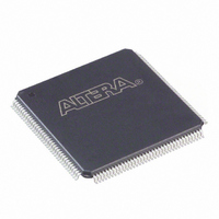
EP1K10TC144-3N Altera, EP1K10TC144-3N Datasheet - Page 15

EP1K10TC144-3N
Manufacturer Part Number
EP1K10TC144-3N
Description
IC ACEX 1K FPGA 10K 144-TQFP
Manufacturer
Altera
Series
ACEX-1K®r
Datasheet
1.EP1K10TC100-3N.pdf
(86 pages)
Specifications of EP1K10TC144-3N
Number Of Logic Elements/cells
576
Number Of Labs/clbs
72
Total Ram Bits
12288
Number Of I /o
92
Number Of Gates
56000
Voltage - Supply
2.375 V ~ 2.625 V
Mounting Type
Surface Mount
Operating Temperature
0°C ~ 85°C
Package / Case
144-TQFP, 144-VQFP
Family Name
ACEX™ 1K
Number Of Usable Gates
10000
Number Of Logic Blocks/elements
576
# I/os (max)
92
Frequency (max)
200MHz
Process Technology
CMOS
Operating Supply Voltage (typ)
2.5V
Logic Cells
576
Ram Bits
12288
Device System Gates
56000
Operating Supply Voltage (min)
2.375V
Operating Supply Voltage (max)
2.625V
Operating Temp Range
0C to 70C
Operating Temperature Classification
Commercial
Mounting
Surface Mount
Pin Count
144
Package Type
TQFP
Lead Free Status / RoHS Status
Lead free / RoHS Compliant
Other names
544-1830
EP1K10TC144-3N
EP1K10TC144-3N
Available stocks
Company
Part Number
Manufacturer
Quantity
Price
Company:
Part Number:
EP1K10TC144-3N
Manufacturer:
ALTERA30
Quantity:
301
Part Number:
EP1K10TC144-3N
Manufacturer:
ALTERA/阿尔特拉
Quantity:
20 000
ACEX 1K Programmable Logic Device Family Data Sheet
Each LAB provides four control signals with programmable inversion
that can be used in all eight LEs. Two of these signals can be used as clocks,
the other two can be used for clear/preset control. The LAB clocks can be
driven by the dedicated clock input pins, global signals, I/O signals, or
internal signals via the LAB local interconnect. The LAB preset and clear
control signals can be driven by the global signals, I/O signals, or internal
signals via the LAB local interconnect. The global control signals are
typically used for global clock, clear, or preset signals because they
provide asynchronous control with very low skew across the device. If
logic is required on a control signal, it can be generated in one or more LEs
in any LAB and driven into the local interconnect of the target LAB. In
addition, the global control signals can be generated from LE outputs.
Logic Element
The LE, the smallest unit of logic in the ACEX 1K architecture, has a
compact size that provides efficient logic utilization. Each LE contains a
4-input LUT, which is a function generator that can quickly compute any
function of four variables. In addition, each LE contains a programmable
13
flipflop with a synchronous clock enable, a carry chain, and a cascade
chain. Each LE drives both the local and the FastTrack Interconnect
routing structure.
Figure 8
shows the ACEX 1K LE.
Altera Corporation
15


