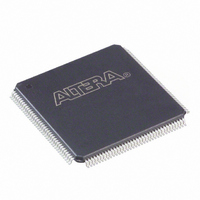
EP1K10TC144-3N Altera, EP1K10TC144-3N Datasheet - Page 7

EP1K10TC144-3N
Manufacturer Part Number
EP1K10TC144-3N
Description
IC ACEX 1K FPGA 10K 144-TQFP
Manufacturer
Altera
Series
ACEX-1K®r
Datasheet
1.EP1K10TC100-3N.pdf
(86 pages)
Specifications of EP1K10TC144-3N
Number Of Logic Elements/cells
576
Number Of Labs/clbs
72
Total Ram Bits
12288
Number Of I /o
92
Number Of Gates
56000
Voltage - Supply
2.375 V ~ 2.625 V
Mounting Type
Surface Mount
Operating Temperature
0°C ~ 85°C
Package / Case
144-TQFP, 144-VQFP
Family Name
ACEX™ 1K
Number Of Usable Gates
10000
Number Of Logic Blocks/elements
576
# I/os (max)
92
Frequency (max)
200MHz
Process Technology
CMOS
Operating Supply Voltage (typ)
2.5V
Logic Cells
576
Ram Bits
12288
Device System Gates
56000
Operating Supply Voltage (min)
2.375V
Operating Supply Voltage (max)
2.625V
Operating Temp Range
0C to 70C
Operating Temperature Classification
Commercial
Mounting
Surface Mount
Pin Count
144
Package Type
TQFP
Lead Free Status / RoHS Status
Lead free / RoHS Compliant
Other names
544-1830
EP1K10TC144-3N
EP1K10TC144-3N
Available stocks
Company
Part Number
Manufacturer
Quantity
Price
Company:
Part Number:
EP1K10TC144-3N
Manufacturer:
ALTERA30
Quantity:
301
Part Number:
EP1K10TC144-3N
Manufacturer:
ALTERA/阿尔特拉
Quantity:
20 000
ACEX 1K Programmable Logic Device Family Data Sheet
The logic array consists of logic array blocks (LABs). Each LAB contains
eight LEs and a local interconnect. An LE consists of a 4-input LUT, a
programmable flipflop, and dedicated signal paths for carry and cascade
functions. The eight LEs can be used to create medium-sized blocks of
logic—such as 8-bit counters, address decoders, or state machines—or
combined across LABs to create larger logic blocks. Each LAB represents
about 96 usable logic gates.
Signal interconnections within ACEX 1K devices (as well as to and from
device pins) are provided by the FastTrack Interconnect routing structure,
which is a series of fast, continuous row and column channels that run the
entire length and width of the device.
Each I/O pin is fed by an I/O element (IOE) located at the end of each row
and column of the FastTrack Interconnect routing structure. Each IOE
contains a bidirectional I/O buffer and a flipflop that can be used as either
an output or input register to feed input, output, or bidirectional signals.
When used with a dedicated clock pin, these registers provide exceptional
performance. As inputs, they provide setup times as low as 1.1 ns and
hold times of 0 ns. As outputs, these registers provide clock-to-output
13
times as low as 2.5 ns. IOEs provide a variety of features, such as JTAG
BST support, slew-rate control, tri-state buffers, and open-drain outputs.
Figure 1
shows a block diagram of the ACEX 1K device architecture. Each
group of LEs is combined into an LAB; groups of LABs are arranged into
rows and columns. Each row also contains a single EAB. The LABs and
EABs are interconnected by the FastTrack Interconnect routing structure.
IOEs are located at the end of each row and column of the FastTrack
Interconnect routing structure.
Altera Corporation
7


