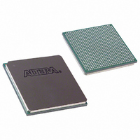
EP2S90F780I4N Altera, EP2S90F780I4N Datasheet - Page 134

EP2S90F780I4N
Manufacturer Part Number
EP2S90F780I4N
Description
IC STRATIX II FPGA 90K 780-FBGA
Manufacturer
Altera
Series
Stratix® IIr
Datasheet
1.EP2S15F484I4N.pdf
(238 pages)
Specifications of EP2S90F780I4N
Number Of Logic Elements/cells
90960
Number Of Labs/clbs
4548
Total Ram Bits
4520488
Number Of I /o
534
Voltage - Supply
1.15 V ~ 1.25 V
Mounting Type
Surface Mount
Operating Temperature
-40°C ~ 100°C
Package / Case
780-FBGA
Family Name
Stratix II
Number Of Logic Blocks/elements
90960
# I/os (max)
534
Frequency (max)
711.24MHz
Process Technology
90nm (CMOS)
Operating Supply Voltage (typ)
1.2V
Logic Cells
90960
Ram Bits
4520488
Operating Supply Voltage (min)
1.15V
Operating Supply Voltage (max)
1.25V
Operating Temp Range
-40C to 100C
Operating Temperature Classification
Industrial
Mounting
Surface Mount
Pin Count
780
Package Type
FC-FBGA
Lead Free Status / RoHS Status
Lead free / RoHS Compliant
Number Of Gates
-
Lead Free Status / Rohs Status
Compliant
Other names
544-2171
Available stocks
Company
Part Number
Manufacturer
Quantity
Price
Company:
Part Number:
EP2S90F780I4N
Manufacturer:
ALTERA
Quantity:
3 000
- Current page: 134 of 238
- Download datasheet (3Mb)
Hot Socketing Feature Implementation in Stratix II Devices
4–4
Stratix II Device Handbook, Volume 1
Figure 4–1. Hot Socketing Circuit Block Diagram for Stratix II Devices
The POR circuit monitors V
stated until the device is in user mode. The weak pull-up resistor (R) from
the I/O pin to V
3.3-V tolerance control circuit permits the I/O pins to be driven by 3.3 V
before V
the I/O pins from driving out when the device is not in user mode. The
hot socket circuit prevents I/O pins from internally powering V
V
powered.
Figure 4–2
I/O buffers. This design ensures that the output buffers do not drive
when V
than V
insertion. There is no current path from signal I/O pins to V
or V
tolerant circuit capacitance.
CCINT
Resistor
Pull-Up
CCPD
Weak
PAD
, and V
CCIO
CCIO
CCIO
during hot insertion. The V
. This also applies for sudden voltage spikes during hot
shows a transistor level cross section of the Stratix II device
is powered before V
and/or V
CCPD
R
CCIO
when driven by external signals before the device is
Output
is present to keep the I/O pins from floating. The
CCINT
CCINT
and/or V
CCINT
voltage level and keeps I/O pins tri-
PAD
Input Buffer
to Logic Array
CCPD
Tolerance
or if the I/O pad voltage is higher
Voltage
Control
leakage current charges the 3.3-V
are powered, and it prevents
Output Enable
Altera Corporation
Hot Socket
Pre-Driver
Output
CCINT
Power On
Monitor
Reset
May 2007
CCIO
or V
,
CCIO
Related parts for EP2S90F780I4N
Image
Part Number
Description
Manufacturer
Datasheet
Request
R

Part Number:
Description:
CYCLONE II STARTER KIT EP2C20N
Manufacturer:
Altera
Datasheet:

Part Number:
Description:
CPLD, EP610 Family, ECMOS Process, 300 Gates, 16 Macro Cells, 16 Reg., 16 User I/Os, 5V Supply, 35 Speed Grade, 24DIP
Manufacturer:
Altera Corporation
Datasheet:

Part Number:
Description:
CPLD, EP610 Family, ECMOS Process, 300 Gates, 16 Macro Cells, 16 Reg., 16 User I/Os, 5V Supply, 15 Speed Grade, 24DIP
Manufacturer:
Altera Corporation
Datasheet:

Part Number:
Description:
Manufacturer:
Altera Corporation
Datasheet:

Part Number:
Description:
CPLD, EP610 Family, ECMOS Process, 300 Gates, 16 Macro Cells, 16 Reg., 16 User I/Os, 5V Supply, 30 Speed Grade, 24DIP
Manufacturer:
Altera Corporation
Datasheet:

Part Number:
Description:
High-performance, low-power erasable programmable logic devices with 8 macrocells, 10ns
Manufacturer:
Altera Corporation
Datasheet:

Part Number:
Description:
High-performance, low-power erasable programmable logic devices with 8 macrocells, 7ns
Manufacturer:
Altera Corporation
Datasheet:

Part Number:
Description:
Classic EPLD
Manufacturer:
Altera Corporation
Datasheet:

Part Number:
Description:
High-performance, low-power erasable programmable logic devices with 8 macrocells, 10ns
Manufacturer:
Altera Corporation
Datasheet:

Part Number:
Description:
Manufacturer:
Altera Corporation
Datasheet:

Part Number:
Description:
Manufacturer:
Altera Corporation
Datasheet:

Part Number:
Description:
Manufacturer:
Altera Corporation
Datasheet:

Part Number:
Description:
CPLD, EP610 Family, ECMOS Process, 300 Gates, 16 Macro Cells, 16 Reg., 16 User I/Os, 5V Supply, 25 Speed Grade, 24DIP
Manufacturer:
Altera Corporation
Datasheet:


