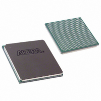
EP2S90F780I4N Altera, EP2S90F780I4N Datasheet - Page 142

EP2S90F780I4N
Manufacturer Part Number
EP2S90F780I4N
Description
IC STRATIX II FPGA 90K 780-FBGA
Manufacturer
Altera
Series
Stratix® IIr
Datasheet
1.EP2S15F484I4N.pdf
(238 pages)
Specifications of EP2S90F780I4N
Number Of Logic Elements/cells
90960
Number Of Labs/clbs
4548
Total Ram Bits
4520488
Number Of I /o
534
Voltage - Supply
1.15 V ~ 1.25 V
Mounting Type
Surface Mount
Operating Temperature
-40°C ~ 100°C
Package / Case
780-FBGA
Family Name
Stratix II
Number Of Logic Blocks/elements
90960
# I/os (max)
534
Frequency (max)
711.24MHz
Process Technology
90nm (CMOS)
Operating Supply Voltage (typ)
1.2V
Logic Cells
90960
Ram Bits
4520488
Operating Supply Voltage (min)
1.15V
Operating Supply Voltage (max)
1.25V
Operating Temp Range
-40C to 100C
Operating Temperature Classification
Industrial
Mounting
Surface Mount
Pin Count
780
Package Type
FC-FBGA
Lead Free Status / RoHS Status
Lead free / RoHS Compliant
Number Of Gates
-
Lead Free Status / Rohs Status
Compliant
Other names
544-2171
Available stocks
Company
Part Number
Manufacturer
Quantity
Price
Company:
Part Number:
EP2S90F780I4N
Manufacturer:
ALTERA
Quantity:
3 000
- Current page: 142 of 238
- Download datasheet (3Mb)
Operating Conditions
5–6
Stratix II Device Handbook, Volume 1
Notes to
(1)
(2)
Notes to
(1)
(2)
V
V
V
V
V
V
V
V
V
V
Table 5–8. 1.8-V I/O Specifications
Table 5–9. 1.5-V I/O Specifications
CCIO
I H
IL
OH
OL
CCIO
I H
IL
OH
OL
Symbol
Symbol
The Stratix II device family’s V
Range of the EIA/JEDEC standard.
This specification is supported across all the programmable drive settings available for this I/O standard as shown
in the Stratix II Architecture chapter in volume 1 of the Stratix II Device Handbook.
The Stratix II device family’s V
Range of the EIA/JEDEC standard.
This specification is supported across all the programmable drive settings available for this I/O standard as shown
in the Stratix II Architecture chapter in volume 1 of the Stratix II Device Handbook.
(1)
(1)
Table
Table
Output supply voltage
High-level input voltage
Low-level input voltage
High-level output voltage
Low-level output voltage
Output supply voltage
High-level input voltage
Low-level input voltage
High-level output voltage
Low-level output voltage
5–8:
5–9:
Parameter
Parameter
Figures 5–1
waveforms, respectively, for all differential I/O standards (LVDS,
LVPECL, and HyperTransport technology).
C C I O
C C I O
voltage level support of 1.8 ± -5% is narrower than defined in the Normal
voltage level support of 1.5 ± -5% is narrower than defined in the Normal
and
I
I
I
I
OH
OL
OH
OL
5–2
= 2 mA
= 2 mA
= –2 mA
= –2 mA
show receiver input and transmitter output
Conditions
Conditions
(2)
(2)
(2)
(2)
0.65 × V
V
0.65 × V
0.75 × V
Minimum
Minimum
CCIO
–0.30
1.425
–0.30
1.71
– 0.45
CCIO
CCIO
CCIO
0.35 × V
V
0.35 × V
0.25 × V
Altera Corporation
Maximum
Maximum
CCIO
1.575
1.89
2.25
0.45
+ 0.30
CCIO
CCIO
CCIO
April 2011
Unit
Unit
V
V
V
V
V
V
V
V
V
V
Related parts for EP2S90F780I4N
Image
Part Number
Description
Manufacturer
Datasheet
Request
R

Part Number:
Description:
CYCLONE II STARTER KIT EP2C20N
Manufacturer:
Altera
Datasheet:

Part Number:
Description:
CPLD, EP610 Family, ECMOS Process, 300 Gates, 16 Macro Cells, 16 Reg., 16 User I/Os, 5V Supply, 35 Speed Grade, 24DIP
Manufacturer:
Altera Corporation
Datasheet:

Part Number:
Description:
CPLD, EP610 Family, ECMOS Process, 300 Gates, 16 Macro Cells, 16 Reg., 16 User I/Os, 5V Supply, 15 Speed Grade, 24DIP
Manufacturer:
Altera Corporation
Datasheet:

Part Number:
Description:
Manufacturer:
Altera Corporation
Datasheet:

Part Number:
Description:
CPLD, EP610 Family, ECMOS Process, 300 Gates, 16 Macro Cells, 16 Reg., 16 User I/Os, 5V Supply, 30 Speed Grade, 24DIP
Manufacturer:
Altera Corporation
Datasheet:

Part Number:
Description:
High-performance, low-power erasable programmable logic devices with 8 macrocells, 10ns
Manufacturer:
Altera Corporation
Datasheet:

Part Number:
Description:
High-performance, low-power erasable programmable logic devices with 8 macrocells, 7ns
Manufacturer:
Altera Corporation
Datasheet:

Part Number:
Description:
Classic EPLD
Manufacturer:
Altera Corporation
Datasheet:

Part Number:
Description:
High-performance, low-power erasable programmable logic devices with 8 macrocells, 10ns
Manufacturer:
Altera Corporation
Datasheet:

Part Number:
Description:
Manufacturer:
Altera Corporation
Datasheet:

Part Number:
Description:
Manufacturer:
Altera Corporation
Datasheet:

Part Number:
Description:
Manufacturer:
Altera Corporation
Datasheet:

Part Number:
Description:
CPLD, EP610 Family, ECMOS Process, 300 Gates, 16 Macro Cells, 16 Reg., 16 User I/Os, 5V Supply, 25 Speed Grade, 24DIP
Manufacturer:
Altera Corporation
Datasheet:


