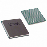
EP2S90F780I4N Altera, EP2S90F780I4N Datasheet - Page 232

EP2S90F780I4N
Manufacturer Part Number
EP2S90F780I4N
Description
IC STRATIX II FPGA 90K 780-FBGA
Manufacturer
Altera
Series
Stratix® IIr
Datasheet
1.EP2S15F484I4N.pdf
(238 pages)
Specifications of EP2S90F780I4N
Number Of Logic Elements/cells
90960
Number Of Labs/clbs
4548
Total Ram Bits
4520488
Number Of I /o
534
Voltage - Supply
1.15 V ~ 1.25 V
Mounting Type
Surface Mount
Operating Temperature
-40°C ~ 100°C
Package / Case
780-FBGA
Family Name
Stratix II
Number Of Logic Blocks/elements
90960
# I/os (max)
534
Frequency (max)
711.24MHz
Process Technology
90nm (CMOS)
Operating Supply Voltage (typ)
1.2V
Logic Cells
90960
Ram Bits
4520488
Operating Supply Voltage (min)
1.15V
Operating Supply Voltage (max)
1.25V
Operating Temp Range
-40C to 100C
Operating Temperature Classification
Industrial
Mounting
Surface Mount
Pin Count
780
Package Type
FC-FBGA
Lead Free Status / RoHS Status
Lead free / RoHS Compliant
Number Of Gates
-
Lead Free Status / Rohs Status
Compliant
Other names
544-2171
Available stocks
Company
Part Number
Manufacturer
Quantity
Price
Company:
Part Number:
EP2S90F780I4N
Manufacturer:
ALTERA
Quantity:
3 000
- Current page: 232 of 238
- Download datasheet (3Mb)
JTAG Timing Specifications
JTAG Timing
Specifications
Figure 5–10. Stratix II JTAG Waveforms
5–96
Stratix II Device Handbook, Volume 1
TMS
TDO
TCK
TDI
t
JCH
t
Figure 5–10
JPZX
Notes to
(1)
(2)
(3)
Notes to
(1)
(2)
t
O U T H A L F J I T T E R
Table 5–100. DQS Phase Offset Delay Per Stage
Table 5–101. DDIO Outputs Half-Period Jitter
t
JCP
The delay settings are linear.
The valid settings for phase offset are -64 to +63 for frequency mode 0 and -32 to
+31 for frequency modes 1, 2, and 3.
The typical value equals the average of the minimum and maximum values.
The worst-case half period is equal to the ideal half period subtracted by the DCD
and half-period jitter values.
The half-period jitter was characterized using a PLL driving DDIO outputs.
Name
t
JCL
Speed Grade
Table
Table
shows the timing requirements for the JTAG signals.
-3
-4
-5
5–100:
5–101:
t
Half-period jitter (PLL driving DDIO outputs)
JPCO
t
JPSU
Description
Min
9
9
9
t
JPH
t
JPXZ
Notes
Max
14
14
15
Notes
(1),
Altera Corporation
(1), (2),
(2)
Max
200
April 2011
(3)
Unit
ps
ps
ps
Unit
ps
Related parts for EP2S90F780I4N
Image
Part Number
Description
Manufacturer
Datasheet
Request
R

Part Number:
Description:
CYCLONE II STARTER KIT EP2C20N
Manufacturer:
Altera
Datasheet:

Part Number:
Description:
CPLD, EP610 Family, ECMOS Process, 300 Gates, 16 Macro Cells, 16 Reg., 16 User I/Os, 5V Supply, 35 Speed Grade, 24DIP
Manufacturer:
Altera Corporation
Datasheet:

Part Number:
Description:
CPLD, EP610 Family, ECMOS Process, 300 Gates, 16 Macro Cells, 16 Reg., 16 User I/Os, 5V Supply, 15 Speed Grade, 24DIP
Manufacturer:
Altera Corporation
Datasheet:

Part Number:
Description:
Manufacturer:
Altera Corporation
Datasheet:

Part Number:
Description:
CPLD, EP610 Family, ECMOS Process, 300 Gates, 16 Macro Cells, 16 Reg., 16 User I/Os, 5V Supply, 30 Speed Grade, 24DIP
Manufacturer:
Altera Corporation
Datasheet:

Part Number:
Description:
High-performance, low-power erasable programmable logic devices with 8 macrocells, 10ns
Manufacturer:
Altera Corporation
Datasheet:

Part Number:
Description:
High-performance, low-power erasable programmable logic devices with 8 macrocells, 7ns
Manufacturer:
Altera Corporation
Datasheet:

Part Number:
Description:
Classic EPLD
Manufacturer:
Altera Corporation
Datasheet:

Part Number:
Description:
High-performance, low-power erasable programmable logic devices with 8 macrocells, 10ns
Manufacturer:
Altera Corporation
Datasheet:

Part Number:
Description:
Manufacturer:
Altera Corporation
Datasheet:

Part Number:
Description:
Manufacturer:
Altera Corporation
Datasheet:

Part Number:
Description:
Manufacturer:
Altera Corporation
Datasheet:

Part Number:
Description:
CPLD, EP610 Family, ECMOS Process, 300 Gates, 16 Macro Cells, 16 Reg., 16 User I/Os, 5V Supply, 25 Speed Grade, 24DIP
Manufacturer:
Altera Corporation
Datasheet:


