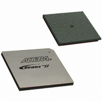
EP2S90F1508I4 Altera, EP2S90F1508I4 Datasheet - Page 120

EP2S90F1508I4
Manufacturer Part Number
EP2S90F1508I4
Description
IC STRATIX II FPGA 90K 1508-FBGA
Manufacturer
Altera
Series
Stratix® IIr
Datasheet
1.EP2S15F484I4N.pdf
(238 pages)
Specifications of EP2S90F1508I4
Number Of Logic Elements/cells
90960
Number Of Labs/clbs
4548
Total Ram Bits
4520488
Number Of I /o
902
Voltage - Supply
1.15 V ~ 1.25 V
Mounting Type
Surface Mount
Operating Temperature
-40°C ~ 100°C
Package / Case
1508-FBGA
Lead Free Status / RoHS Status
Contains lead / RoHS non-compliant
Number Of Gates
-
Other names
544-1923
EP2S90F1508I4
EP2S90F1508I4
Available stocks
Company
Part Number
Manufacturer
Quantity
Price
Company:
Part Number:
EP2S90F1508I4
Manufacturer:
ALTERA
Quantity:
3 000
Company:
Part Number:
EP2S90F1508I4N
Manufacturer:
ALTERA
Quantity:
586
- Current page: 120 of 238
- Download datasheet (3Mb)
Configuration
3–6
Stratix II Device Handbook, Volume 1
The PLL_ENA pin and the configuration input pins
dual buffer design: a 3.3-V/2.5-V input buffer and a 1.8-V/1.5-V input
buffer. The VCCSEL input pin selects which input buffer is used. The 3.3-
V/2.5-V input buffer is powered by V
buffer is powered by V
VCCSEL is sampled during power-up. Therefore, the VCCSEL setting
cannot change on the fly or during a reconfiguration. The VCCSEL input
buffer is powered by V
A logic high VCCSEL connection selects the 1.8-V/1.5-V input buffer, and
a logic low selects the 3.3-V/2.5-V input buffer. VCCSEL should be set to
comply with the logic levels driven out of the configuration device or
MAX
If you need to support configuration input voltages of 3.3 V/2.5 V, you
should set the VCCSEL to a logic low; you can set the V
bank that contains the configuration inputs to any supported voltage. If
nSTATUS
used as an input)
nCONFIG
CONF_DONE
(when used as an
input)
DATA[7..0]
nCE
DCLK
as an input)
CS
nWS
nRS
nCS
CLKUSR
DEV_OE
DEV_CLRn
RUnLU
PLL_ENA
Table 3–4. Pins Affected by the Voltage Level at VCCSEL
®
(when used
II/microprocessor.
Pin
(when
3.3/2.5-V input buffer is
selected. Input buffer is
powered by V
VCCSEL = LOW (connected
CCIO
CCINT
.
Table 3–4
to GND)
and must be hardwired to V
C C P D
.
shows the pins affected by VCCSEL.
CCPD,
while the 1.8-V/1.5-V input
1.8/1.5-V input buffer is
selected. Input buffer is
powered by V
bank.
VCCSEL = HIGH (connected
(Table
Altera Corporation
CCIO
to V
CCPD
3–4) have a
C C I O
CCPD
of the I/O
or ground.
)
of the I/O
May 2007
Related parts for EP2S90F1508I4
Image
Part Number
Description
Manufacturer
Datasheet
Request
R

Part Number:
Description:
CYCLONE II STARTER KIT EP2C20N
Manufacturer:
Altera
Datasheet:

Part Number:
Description:
CPLD, EP610 Family, ECMOS Process, 300 Gates, 16 Macro Cells, 16 Reg., 16 User I/Os, 5V Supply, 35 Speed Grade, 24DIP
Manufacturer:
Altera Corporation
Datasheet:

Part Number:
Description:
CPLD, EP610 Family, ECMOS Process, 300 Gates, 16 Macro Cells, 16 Reg., 16 User I/Os, 5V Supply, 15 Speed Grade, 24DIP
Manufacturer:
Altera Corporation
Datasheet:

Part Number:
Description:
Manufacturer:
Altera Corporation
Datasheet:

Part Number:
Description:
CPLD, EP610 Family, ECMOS Process, 300 Gates, 16 Macro Cells, 16 Reg., 16 User I/Os, 5V Supply, 30 Speed Grade, 24DIP
Manufacturer:
Altera Corporation
Datasheet:

Part Number:
Description:
High-performance, low-power erasable programmable logic devices with 8 macrocells, 10ns
Manufacturer:
Altera Corporation
Datasheet:

Part Number:
Description:
High-performance, low-power erasable programmable logic devices with 8 macrocells, 7ns
Manufacturer:
Altera Corporation
Datasheet:

Part Number:
Description:
Classic EPLD
Manufacturer:
Altera Corporation
Datasheet:

Part Number:
Description:
High-performance, low-power erasable programmable logic devices with 8 macrocells, 10ns
Manufacturer:
Altera Corporation
Datasheet:

Part Number:
Description:
Manufacturer:
Altera Corporation
Datasheet:

Part Number:
Description:
Manufacturer:
Altera Corporation
Datasheet:

Part Number:
Description:
Manufacturer:
Altera Corporation
Datasheet:

Part Number:
Description:
CPLD, EP610 Family, ECMOS Process, 300 Gates, 16 Macro Cells, 16 Reg., 16 User I/Os, 5V Supply, 25 Speed Grade, 24DIP
Manufacturer:
Altera Corporation
Datasheet:


