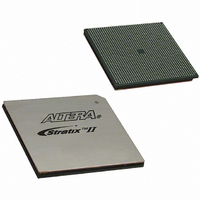
EP2S90F1508I4 Altera, EP2S90F1508I4 Datasheet - Page 135

EP2S90F1508I4
Manufacturer Part Number
EP2S90F1508I4
Description
IC STRATIX II FPGA 90K 1508-FBGA
Manufacturer
Altera
Series
Stratix® IIr
Datasheet
1.EP2S15F484I4N.pdf
(238 pages)
Specifications of EP2S90F1508I4
Number Of Logic Elements/cells
90960
Number Of Labs/clbs
4548
Total Ram Bits
4520488
Number Of I /o
902
Voltage - Supply
1.15 V ~ 1.25 V
Mounting Type
Surface Mount
Operating Temperature
-40°C ~ 100°C
Package / Case
1508-FBGA
Lead Free Status / RoHS Status
Contains lead / RoHS non-compliant
Number Of Gates
-
Other names
544-1923
EP2S90F1508I4
EP2S90F1508I4
Available stocks
Company
Part Number
Manufacturer
Quantity
Price
Company:
Part Number:
EP2S90F1508I4
Manufacturer:
ALTERA
Quantity:
3 000
Company:
Part Number:
EP2S90F1508I4N
Manufacturer:
ALTERA
Quantity:
586
Figure 4–2. Transistor Level Diagram of FPGA Device I/O Buffers
Notes to
(1)
(2)
Power-On Reset
Circuitry
Altera Corporation
May 2007
This is the logic array signal or the larger of either the V
This is the larger of either the V
Figure
4–2:
n+
Logic Array
Stratix II devices have a POR circuit to keep the whole device system in
reset state until the power supply voltage levels have stabilized during
power-up. The POR circuit monitors the V
levels and tri-states all the user I/O pins while V
normal user levels are reached. The POR circuitry also ensures that all
eight I/O bank V
V
triggered. After the Stratix II device enters user mode, the POR circuit
continues to monitor the V
condition during user mode can be detected. If there is a V
sag below the Stratix II operational level during user mode, the POR
circuit resets the device.
When power is applied to a Stratix II device, a power-on-reset event
occurs if V
period of time (specified as a maximum V
V
dedicated input pin (PORSEL) to select POR delay times of 12 or 100 ms
during power-up. When the PORSEL pin is connected to ground, the POR
time is 100 ms. When the PORSEL pin is connected to V
is 12 ms.
p-well
Signal
CCINT
CC
CCIO
rise time for Stratix II device is 100 ms. Stratix II devices provide a
voltage, reach an acceptable level before configuration is
or V
n+
CC
PAD
reaches the recommended operating range within a certain
signal.
V
CCIO
PAD
voltages, V
CCIO
p+
CCINT
or V
PAD
(1)
voltage level so that a brown-out
CCPD
signal.
Stratix II Device Handbook, Volume 1
n-well
voltage, as well as the logic array
V
CCIO
p+
Hot Socketing & Power-On Reset
CCINT
CC
rise time). The maximum
, V
(2)
n+
CC
CCIO
p-substrate
is ramping up until
, and V
CC
, the POR time
CCINT
CCPD
voltage
voltage
4–5


