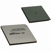
EP2S90F1508I4 Altera, EP2S90F1508I4 Datasheet - Page 157

EP2S90F1508I4
Manufacturer Part Number
EP2S90F1508I4
Description
IC STRATIX II FPGA 90K 1508-FBGA
Manufacturer
Altera
Series
Stratix® IIr
Datasheet
1.EP2S15F484I4N.pdf
(238 pages)
Specifications of EP2S90F1508I4
Number Of Logic Elements/cells
90960
Number Of Labs/clbs
4548
Total Ram Bits
4520488
Number Of I /o
902
Voltage - Supply
1.15 V ~ 1.25 V
Mounting Type
Surface Mount
Operating Temperature
-40°C ~ 100°C
Package / Case
1508-FBGA
Lead Free Status / RoHS Status
Contains lead / RoHS non-compliant
Number Of Gates
-
Other names
544-1923
EP2S90F1508I4
EP2S90F1508I4
Available stocks
Company
Part Number
Manufacturer
Quantity
Price
Company:
Part Number:
EP2S90F1508I4
Manufacturer:
ALTERA
Quantity:
3 000
Company:
Part Number:
EP2S90F1508I4N
Manufacturer:
ALTERA
Quantity:
586
- Current page: 157 of 238
- Download datasheet (3Mb)
Altera Corporation
April 2011
Preliminary status means the timing model is subject to change. Initially,
timing numbers are created using simulation results, process data, and
other known parameters. These tests are used to make the preliminary
numbers as close to the actual timing parameters as possible.
Final timing numbers are based on actual device operation and testing.
These numbers reflect the actual performance of the device under
worst-case voltage and junction temperature conditions.
I/O Timing Measurement Methodology
Altera characterizes timing delays at the worst-case process, minimum
voltage, and maximum temperature for input register setup time (t
and hold time (t
to calculate t
Figure 5–3
Table 5–33. Stratix II Device Timing Model Status
t
t
SU
H
= – data delay from input pin to input register
EP2S130
EP2S180
= + data delay from input pin to input register
EP2S15
EP2S30
EP2S60
EP2S90
Device
+ micro setup time of the input register
– clock delay from input pin to input register
+ micro hold time of the input register
+ clock delay from input pin to input register
shows the setup and hold timing diagram for input registers.
SU
and t
H
). The Quartus II software uses the following equations
H
timing for Stratix II devices input signals.
Preliminary
Stratix II Device Handbook, Volume 1
DC & Switching Characteristics
Final
v
v
v
v
v
v
SU
5–21
)
Related parts for EP2S90F1508I4
Image
Part Number
Description
Manufacturer
Datasheet
Request
R

Part Number:
Description:
CYCLONE II STARTER KIT EP2C20N
Manufacturer:
Altera
Datasheet:

Part Number:
Description:
CPLD, EP610 Family, ECMOS Process, 300 Gates, 16 Macro Cells, 16 Reg., 16 User I/Os, 5V Supply, 35 Speed Grade, 24DIP
Manufacturer:
Altera Corporation
Datasheet:

Part Number:
Description:
CPLD, EP610 Family, ECMOS Process, 300 Gates, 16 Macro Cells, 16 Reg., 16 User I/Os, 5V Supply, 15 Speed Grade, 24DIP
Manufacturer:
Altera Corporation
Datasheet:

Part Number:
Description:
Manufacturer:
Altera Corporation
Datasheet:

Part Number:
Description:
CPLD, EP610 Family, ECMOS Process, 300 Gates, 16 Macro Cells, 16 Reg., 16 User I/Os, 5V Supply, 30 Speed Grade, 24DIP
Manufacturer:
Altera Corporation
Datasheet:

Part Number:
Description:
High-performance, low-power erasable programmable logic devices with 8 macrocells, 10ns
Manufacturer:
Altera Corporation
Datasheet:

Part Number:
Description:
High-performance, low-power erasable programmable logic devices with 8 macrocells, 7ns
Manufacturer:
Altera Corporation
Datasheet:

Part Number:
Description:
Classic EPLD
Manufacturer:
Altera Corporation
Datasheet:

Part Number:
Description:
High-performance, low-power erasable programmable logic devices with 8 macrocells, 10ns
Manufacturer:
Altera Corporation
Datasheet:

Part Number:
Description:
Manufacturer:
Altera Corporation
Datasheet:

Part Number:
Description:
Manufacturer:
Altera Corporation
Datasheet:

Part Number:
Description:
Manufacturer:
Altera Corporation
Datasheet:

Part Number:
Description:
CPLD, EP610 Family, ECMOS Process, 300 Gates, 16 Macro Cells, 16 Reg., 16 User I/Os, 5V Supply, 25 Speed Grade, 24DIP
Manufacturer:
Altera Corporation
Datasheet:


