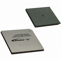
EP2S90F1508I4 Altera, EP2S90F1508I4 Datasheet - Page 56

EP2S90F1508I4
Manufacturer Part Number
EP2S90F1508I4
Description
IC STRATIX II FPGA 90K 1508-FBGA
Manufacturer
Altera
Series
Stratix® IIr
Datasheet
1.EP2S15F484I4N.pdf
(238 pages)
Specifications of EP2S90F1508I4
Number Of Logic Elements/cells
90960
Number Of Labs/clbs
4548
Total Ram Bits
4520488
Number Of I /o
902
Voltage - Supply
1.15 V ~ 1.25 V
Mounting Type
Surface Mount
Operating Temperature
-40°C ~ 100°C
Package / Case
1508-FBGA
Lead Free Status / RoHS Status
Contains lead / RoHS non-compliant
Number Of Gates
-
Other names
544-1923
EP2S90F1508I4
EP2S90F1508I4
Available stocks
Company
Part Number
Manufacturer
Quantity
Price
Company:
Part Number:
EP2S90F1508I4
Manufacturer:
ALTERA
Quantity:
3 000
Company:
Part Number:
EP2S90F1508I4N
Manufacturer:
ALTERA
Quantity:
586
PLLs & Clock Networks
PLLs & Clock
Networks
2–48
Stratix II Device Handbook, Volume 1
Stratix II devices provide a hierarchical clock structure and multiple PLLs
with advanced features. The large number of clocking resources in
combination with the clock synthesis precision provided by enhanced
and fast PLLs provides a complete clock management solution.
Global & Hierarchical Clocking
Stratix II devices provide 16 dedicated global clock networks and
32 regional clock networks (eight per device quadrant). These clocks are
organized into a hierarchical clock structure that allows for up to
24 clocks per device region with low skew and delay. This hierarchical
clocking scheme provides up to 48 unique clock domains in Stratix II
devices.
There are 16 dedicated clock pins (CLK[15..0]) to drive either the global
or regional clock networks. Four clock pins drive each side of the device,
as shown in
PLL outputs can also drive the global and regional clock networks. Each
global and regional clock has a clock control block, which controls the
selection of the clock source and dynamically enables/disables the clock
to reduce power consumption.
features.
Global Clock Network
These clocks drive throughout the entire device, feeding all device
quadrants. The global clock networks can be used as clock sources for all
resources in the device-IOEs, ALMs, DSP blocks, and all memory blocks.
These resources can also be used for control signals, such as clock enables
and synchronous or asynchronous clears fed from the external pin. The
Note to
(1)
Number per device
Number available per
quadrant
Sources
Dynamic clock source
selection
Dynamic enable/disable
Table 2–8. Global & Regional Clock Features
Dynamic source clock selection is supported for selecting between CLKp pins and
PLL outputs only.
Table
Feature
Figures 2–31
2–8:
and 2–32. Internal logic and enhanced and fast
CLK pins, PLL outputs,
or internal logic
Table 2–8
Global Clocks
v
v
16
16
(1)
shows global and regional clock
CLK pins, PLL outputs,
or internal logic
Regional Clocks
Altera Corporation
v
32
8
May 2007


