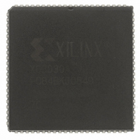
XC3030A-7PC84C Xilinx Inc, XC3030A-7PC84C Datasheet - Page 47

XC3030A-7PC84C
Manufacturer Part Number
XC3030A-7PC84C
Description
IC LOGIC CL ARRAY 3000GAT 84PLCC
Manufacturer
Xilinx Inc
Series
XC3000A/Lr
Datasheet
1.XC3190A-3PC84C.pdf
(76 pages)
Specifications of XC3030A-7PC84C
Number Of Labs/clbs
100
Total Ram Bits
22176
Number Of I /o
74
Number Of Gates
2000
Voltage - Supply
4.75 V ~ 5.25 V
Mounting Type
Surface Mount
Operating Temperature
0°C ~ 85°C
Package / Case
84-LCC (J-Lead)
Lead Free Status / RoHS Status
Contains lead / RoHS non-compliant
Number Of Logic Elements/cells
-
Other names
122-1018
Available stocks
Company
Part Number
Manufacturer
Quantity
Price
Company:
Part Number:
XC3030A-7PC84C
Manufacturer:
XILINX
Quantity:
181
Part Number:
XC3030A-7PC84C
Manufacturer:
XILINX/赛灵思
Quantity:
20 000
XC3000L CLB Switching Characteristics Guidelines
Testing of the switching parameters is modeled after testing methods specified by MIL-M-38510/605. All devices are 100%
functionally tested. Since many internal timing parameters cannot be measured directly, they are derived from benchmark
timing patterns. The following guidelines reflect worst-case values over the recommended operating conditions. For more
detailed, more precise, and more up-to-date timing information, use the values provided by the timing calculator and used
in the simulator.
Notes:
November 9, 1998 (Version 3.1)
Combinatorial Delay
Sequential delay
Set-up time before clock K
Hold Time after clock K
Clock
Reset Direct (RD)
Global Reset (RESET Pad)
Logic Variables
Clock k to outputs X or Y
Clock k to outputs X or Y when Q is returned
through function generators F or G to drive X or Y
Logic Variables
Data In
Enable Clock
Logic Variables
Data In
Enable Clock
Clock High time
Clock Low time
Max. flip-flop toggle rate
RD width
delay from RD to outputs X or Y
RESET width (Low)
delay from RESET pad to outputs X or Y
1. Timing is based on the XC3042L, for other devices see timing calculator.
2. The CLB K to Q output delay (T
Data In hold time requirement (T
R
Product Obsolete or Under Obsolescence
FG Mode
F and FGM Mode
EC
A, B, C, D, E
A, B, C, D, E, to outputs X or Y
FG Mode
F and FGM Mode
FG Mode
F and FGM Mode
A, B, C, D, E
DI
DI
EC
2
1
Description
CKO
CKDI
, #8) of any CLB, plus the shortest possible interconnect delay, is always longer than the
, #5) of any CLB on the same die.
XC3000 Series Field Programmable Gate Arrays
11
12
13
1
8
2
4
6
9
3
5
7
Speed Grade
Symbol
T
T
T
T
T
T
T
T
T
F
T
T
T
T
T
ECCK
CKEC
T
DICK
CKDI
RPW
MRW
MRQ
CKO
QLO
CLK
ICK
CKI
RIO
ILO
CH
CL
80.0
16.0
Min
5.0
5.8
5.0
6.0
2.0
2.0
5.0
5.0
7.0
7.0
0
-8
Max
14.0
14.8
23.0
6.7
7.5
7.5
Units
MHz
ns
ns
ns
ns
ns
ns
ns
ns
ns
ns
ns
ns
ns
ns
ns
ns
ns
ns
7-49
7


