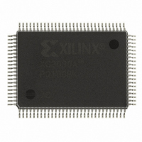
XC3030A-7PQ100C Xilinx Inc, XC3030A-7PQ100C Datasheet - Page 36

XC3030A-7PQ100C
Manufacturer Part Number
XC3030A-7PQ100C
Description
IC LOGIC CL ARRAY 3000GAT 100PQF
Manufacturer
Xilinx Inc
Series
XC3000A/Lr
Datasheet
1.XC3190A-3PC84C.pdf
(76 pages)
Specifications of XC3030A-7PQ100C
Number Of Labs/clbs
100
Total Ram Bits
22176
Number Of I /o
80
Number Of Gates
2000
Voltage - Supply
4.75 V ~ 5.25 V
Mounting Type
Surface Mount
Operating Temperature
0°C ~ 85°C
Package / Case
100-BQFP
Case
QFP100
Dc
98+
Lead Free Status / RoHS Status
Contains lead / RoHS non-compliant
Number Of Logic Elements/cells
-
Other names
122-1019
Available stocks
Company
Part Number
Manufacturer
Quantity
Price
Company:
Part Number:
XC3030A-7PQ100C
Manufacturer:
XILINX
Quantity:
181
XC3000 Series Field Programmable Gate Arrays
Pin Descriptions
Permanently Dedicated Pins
V
Two to eight (depending on package type) connections to
the positive V supply voltage. All must be connected.
GND
Two to eight (depending on package type) connections to
ground. All must be connected.
PWRDWN
A Low on this CMOS-compatible input stops all internal
activity, but retains configuration. All flip-flops and latches
are reset, all outputs are 3-stated, and all inputs are inter-
preted as High, independent of their actual level. When
PWDWN returns High, the FPGA becomes operational
with DONE Low for two cycles of the internal 1-MHz clock.
Before and during configuration, PWRDWN must be High.
If not used, PWRDWN must be tied to V
RESET
This is an active Low input which has three functions.
Prior to the start of configuration, a Low input will delay the
start of the configuration process. An internal circuit senses
the application of power and begins a minimal time-out
cycle. When the time-out and RESET are complete, the
levels of the M lines are sampled and configuration begins.
If RESET is asserted during a configuration, the FPGA is
re-initialized and restarts the configuration at the termina-
tion of RESET.
If RESET is asserted after configuration is complete, it pro-
vides a global asynchronous RESET of all IOB and CLB
storage elements of the FPGA.
CCLK
During configuration, Configuration Clock is an output of an
FPGA in Master mode or Peripheral mode, but an input in
Slave mode. During Readback, CCLK is a clock input for
shifting configuration data out of the FPGA.
CCLK drives dynamic circuitry inside the FPGA. The Low
time may, therefore, not exceed a few microseconds. When
used as an input, CCLK must be “parked High”. An internal
pull-up resistor maintains High when the pin is not being
driven.
DONE/PROG (D/P)
DONE is an open-drain output, configurable with or without
an internal pull-up resistor of 2 to 8 k . At the completion of
configuration, the FPGA circuitry becomes active in a syn-
chronous order; DONE is programmed to go active High
one cycle either before or after the outputs go active.
7-38
CC
Product Obsolete or Under Obsolescence
CC
.
Once configuration is done, a High-to-Low transition of this
pin will cause an initialization of the FPGA and start a
reconfiguration.
M0/RTRIG
As Mode 0, this input is sampled on power-on to determine
the power-on delay (2
is Low). Before the start of configuration, this input is again
sampled together with M1, M2 to determine the configura-
tion mode to be used.
A Low-to-High input transition, after configuration is com-
plete, acts as a Read Trigger and initiates a Readback of
configuration and storage-element data clocked by CCLK.
By selecting the appropriate Readback option when gener-
ating the bitstream, this operation may be limited to a single
Readback, or be inhibited altogether.
M1/RDATA
As Mode 1, this input and M0, M2 are sampled before the
start of configuration to establish the configuration mode to
be used. If Readback is never used, M1 can be tied directly
to ground or V
5-k
RDATA output.
As an active-Low Read Data, after configuration is com-
plete, this pin is the output of the Readback data.
User I/O Pins That Can Have Special
Functions
M2
During configuration, this input has a weak pull-up resistor.
Together with M0 and M1, it is sampled before the start of
configuration to establish the configuration mode to be
used. After configuration, this pin is a user-programmable
I/O pin.
HDC
During configuration, this output is held at a High level to
indicate that configuration is not yet complete. After config-
uration, this pin is a user-programmable I/O pin.
LDC
During Configuration, this output is held at a Low level to
indicate that the configuration is not yet complete. After
configuration, this pin is a user-programmable I/O pin. LDC
is particularly useful in Master mode as a Low enable for an
EPROM, but it must then be programmed as a High after
configuration.
INIT
This is an active Low open-drain output with a weak pull-up
and is held Low during the power stabilization and internal
clearing of the configuration memory. It can be used to indi-
cate status to a configuring microprocessor or, as a wired
resistor to ground or V
CC
. If Readback is ever used, M1 must use a
14
cycles if M0 is High, 2
November 9, 1998 (Version 3.1)
CC
, to accommodate the
16
cycles if M0
R


