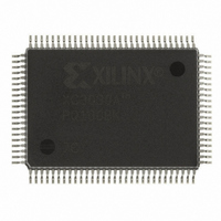
XC3030A-7PQ100C Xilinx Inc, XC3030A-7PQ100C Datasheet - Page 45

XC3030A-7PQ100C
Manufacturer Part Number
XC3030A-7PQ100C
Description
IC LOGIC CL ARRAY 3000GAT 100PQF
Manufacturer
Xilinx Inc
Series
XC3000A/Lr
Datasheet
1.XC3190A-3PC84C.pdf
(76 pages)
Specifications of XC3030A-7PQ100C
Number Of Labs/clbs
100
Total Ram Bits
22176
Number Of I /o
80
Number Of Gates
2000
Voltage - Supply
4.75 V ~ 5.25 V
Mounting Type
Surface Mount
Operating Temperature
0°C ~ 85°C
Package / Case
100-BQFP
Case
QFP100
Dc
98+
Lead Free Status / RoHS Status
Contains lead / RoHS non-compliant
Number Of Logic Elements/cells
-
Other names
122-1019
Available stocks
Company
Part Number
Manufacturer
Quantity
Price
Company:
Part Number:
XC3030A-7PQ100C
Manufacturer:
XILINX
Quantity:
181
XC3000L Switching Characteristics
Xilinx maintains test specifications for each product as controlled documents. To insure the use of the most recently released
device performance parameters, please request a copy of the current test-specification revision.
XC3000L Operating Conditions
Notes:
XC3000L DC Characteristics Over Operating Conditions
Notes:
November 9, 1998 (Version 3.1)
Symbol
Symbol
V
I
CCPD
I
V
V
V
V
V
I
CCPD
I
V
CCO
C
V
T
RLL
RIN
I
CC
OH
OH
OL
OL
IL
IN
IH
IN
IL
1. At junction temperatures above those listed as Operating Conditions, all delay parameters increase by 0.3% per C.
2. Although the present (1996) devices operate over the full supply voltage range from 3.0 to 5.25 V, Xilinx reserves the right to
1. With no output current loads, no active input or Longline pull-up resistors, all package pins at V
2. Total continuous output sink current may not exceed 100 mA per ground pin. Total continuous output source may not exceed
3. Not tested. Allows an undriven pin to float High. For any other purpose, use an external pull-up.
restrict operation to the 3.0 to 3.6 V range later, when smaller device geometries might preclude operation at 5V. Operating
conditions are guaranteed in the 3.0 – 3.6 V V
device configured with a tie option. I
100 mA per V
R
Supply voltage relative to GND Commercial 0 C to +85 C junction
High-level input voltage — TTL configuration
Low-level input voltage — TTL configuration
Input signal transition time
High-level output voltage (@ I
Low-level output voltage (@ I
High-level output voltage (@ I
Low-level output voltage (@ I
Power-down supply voltage (PWRDWN must be Low)
Power-down supply current (V
Quiescent FPGA supply current in addition to I
Input Leakage Current
Input capacitance, all packages except PGA175
Input capacitance, PGA 175
Pad pull-up (when selected) @ V
Horizontal Longline pull-up (when selected) @ logic Low
Chip thresholds programmed as CMOS levels
(sample tested)
All Pins except XTL1 and XTL2
XTL1 and XTL2
(sample tested)
All Pins except XTL1 and XTL2
XTL1 and XTL2
CC
Product Obsolete or Under Obsolescence
pin. The number of ground pins varies from the XC3020L to the XC3090L.
CCO
Description
OL
OL
Description
OH
OH
is in addition to I
CC(MAX)
= 4.0 mA, V
= 4.0 mA, V
= –4.0 mA, V
= –4.0 mA, V
IN
CC
= 0 V
range.
@ T
3
XC3000 Series Field Programmable Gate Arrays
MAX
CC
CC
CCPD
CC
CC
CCPD
)
min)
min)
.
min)
min)
1
Min
-0.3
V
3.0
2.0
CC
2.40
2.30
0.01
Min
–10
CC
-0.2
or GND, and the FPGA
V
CC
Max
250
3.6
0.8
Max
0.40
0.17
2.50
+10
0.2
10
20
10
15
15
20
+0.3
Units
Units
mA
mA
ns
pF
pF
pF
pF
V
V
V
V
V
V
V
V
A
A
A
7-47
7


