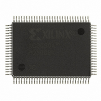
XC3030A-7PQ100C Xilinx Inc, XC3030A-7PQ100C Datasheet - Page 52

XC3030A-7PQ100C
Manufacturer Part Number
XC3030A-7PQ100C
Description
IC LOGIC CL ARRAY 3000GAT 100PQF
Manufacturer
Xilinx Inc
Series
XC3000A/Lr
Datasheet
1.XC3190A-3PC84C.pdf
(76 pages)
Specifications of XC3030A-7PQ100C
Number Of Labs/clbs
100
Total Ram Bits
22176
Number Of I /o
80
Number Of Gates
2000
Voltage - Supply
4.75 V ~ 5.25 V
Mounting Type
Surface Mount
Operating Temperature
0°C ~ 85°C
Package / Case
100-BQFP
Case
QFP100
Dc
98+
Lead Free Status / RoHS Status
Contains lead / RoHS non-compliant
Number Of Logic Elements/cells
-
Other names
122-1019
Available stocks
Company
Part Number
Manufacturer
Quantity
Price
Company:
Part Number:
XC3030A-7PQ100C
Manufacturer:
XILINX
Quantity:
181
XC3000 Series Field Programmable Gate Arrays
XC3100A Absolute Maximum Ratings
Note:
XC3100A Global Buffer Switching Characteristics Guidelines
Note:
7-54
Global and Alternate Clock Distribution
Either: Normal IOB input pad through clock buffer
Or: Fast (CMOS only) input pad through clock
TBUF driving a Horizontal Longline (L.L.)
BIDI
Symbol
T
T
V
to any CLB or IOB clock input
I to L.L. while T is Low (buffer active)
T to L.L. active and valid with single pull-up resistor
T to L.L. active and valid with pair of pull-up resistors
T to L.L. High with single pull-up resistor
T to L.L. High with pair of pull-up resistors
Bidirectional buffer delay
V
V
buffer to any CLB or IOB clock input
STG
SOL
T
CC
TS
IN
1. Timing is based on the XC3142A, for other devices see timing calculator.
J
Stresses beyond those listed under Absolute Maximum Ratings may cause permanent damage to the device. These are
stress ratings only, and functional operation of the device at these or any other conditions beyond those listed under
Recommended Operating Conditions is not implied. Exposure to Absolute Maximum Ratings conditions for extended
periods of time may affect device reliability.
The use of two pull-up resistors per longline, available on other XC3000 devices, is not a valid design option for XC3100A
devices.
Supply voltage relative to GND
Input voltage with respect to GND
Voltage applied to 3-state output
Storage temperature (ambient)
Maximum soldering temperature (10 s @ 1/16 in.)
Junction temperature plastic
Junction temperature ceramic
Product Obsolete or Under Obsolescence
Description
1
1
Description
(XC3100)
(XC3100A)
Speed Grade
Symbol
T
T
T
T
T
T
T
T
T
PIDC
PUS
PUF
BIDI
PID
ON
ON
IO
IO
Max
13.5
10.5
6.5
5.1
3.7
3.6
5.0
6.5
1.2
-4
Max
11.4
5.6
4.3
3.1
3.1
4.2
5.7
8.8
1.0
-3
November 9, 1998 (Version 3.1)
–0.5 to V
–0.5 to V
11.4
Max
–0.5 to +7.0
–65 to +150
4.7
3.7
3.1
4.2
5.7
8.1
0.9
-2
+260
+125
+150
CC
CC
Max
10.4
0.85
4.3
3.5
2.9
4.0
5.5
7.1
-1
+0.5
+0.5
Prelim
Max
0.75
-09
3.9
3.1
2.1
3.1
4.6
8.9
5.9
Units
V
V
V
C
C
C
C
Units
ns
ns
ns
ns
ns
ns
ns
ns
ns
R


