CY7C68013-56PVC Cypress Semiconductor Corp, CY7C68013-56PVC Datasheet
CY7C68013-56PVC
Specifications of CY7C68013-56PVC
Available stocks


Related parts for CY7C68013-56PVC


CY7C68013-56PVC Summary of contents
Page 1
... CY7C68013 EZ-USB FX2™ USB Microcontroller High-speed USB Peripheral Controller Cypress Semiconductor Corporation Document #: 38-08012 Rev. *C • 3901 North First Street • San Jose CY7C68013 , CA 95134 • 408-943-2600 Revised December 19, 2002 ...
Page 2
... GPIF ........................................................................................................................................ 16 3.15 USB Uploads and Downloads ................................................................................................. 17 3.16 Autopointer Access ................................................................................................................. 17 2 3.17 I C-compatible Controller ........................................................................................................ 17 4.0 PIN ASSIGNMENTS ...................................................................................................................... 18 4.1 CY7C68013 Pin Descriptions ................................................................................................... 24 5.0 REGISTER SUMMARY .................................................................................................................. 31 6.0 ABSOLUTE MAXIMUM RATINGS ................................................................................................ 37 7.0 OPERATING CONDITIONS ........................................................................................................... 37 8.0 DC CHARACTERISTICS ............................................................................................................... 37 8.1 USB Transceiver ....................................................................................................................... 37 9.0 AC ELECTRICAL CHARACTERISTICS ....................................................................................... 38 9.1 USB Transceiver ....................................................................................................................... 38 9 ...
Page 3
... ORDERING INFORMATION ........................................................................................................ 46 11.0 PACKAGE DIAGRAMS ............................................................................................................... 47 12.0 PCB LAYOUT RECOMMENDATIONS ........................................................................................ 50 13.0 QUAD FLAT PACKAGE NO LEADS (QFN) PACKAGE DESIGN NOTES ................................ 50 Document #: 38-08012 Rev. *C CY7C68013 Page ...
Page 4
... Figure 4-2. CY7C68013 128-pin TQFP Pin Assignment ....................................................................... 20 Figure 4-3. CY7C68013 100-pin TQFP Pin Assignment ....................................................................... 21 Figure 4-4. CY7C68013 56-pin SSOP Pin Assignment ......................................................................... 22 Figure 4-5. CY7C68013 56-pin QFN Pin Assignment ........................................................................... 23 Figure 9-1. Program Memory Read Timing Diagram............................................................................. 38 Figure 9-2. Data Memory Read Timing Diagram ................................................................................... 39 Figure 9-3 ...
Page 5
... Table 9-14. Slave FIFO Asynchronous Packet End Strobe Parameters .............................................. 45 Table 9-15. Slave FIFO Output Enable Parameters ............................................................................. 45 Table 9-16. Slave FIFO Address to Flags/Data Parameters ................................................................ 46 Table 9-17. Slave FIFO Synchronous Address Parameters ................................................................. 46 Table 9-18. Slave FIFO Asynchronous Address Parameters ............................................................... 46 Table 10-1. Ordering Information .......................................................................................................... 46 Document #: 38-08012 Rev. *C LIST OF TABLES CY7C68013 Page ...
Page 6
... MHz, /2.0 four clocks/cycle CY 8.5 kB Smart RAM USB 1.1/2.0 Engine “Soft Configuration” Easy firmware changes Figure 1-1. Block Diagram CY7C68013 Compatible Master Abundant I/O Additional I/Os (24) including two USARTS General ADDR (9) programmable I/F to ASIC/DSP or bus GPIF standards such as RDY (6) ATAPI, EPP, etc ...
Page 7
... High speed, with a signaling bit rate of 480 Mbps FX2 does not support the low-speed signaling mode of 1.5 Mbps. 3.2 8051 Microprocessor The 8051 microprocessor embedded in the FX2 family has 256 bytes of register RAM, an expanded interrupt system, three timer/counters, and two USARTs. Document #: 38-08012 Rev. *C CY7C68013 Page ...
Page 8
... These signals must be pulled up to 3.3V, even 3.4 Buses All packages 16-bit “FIFO” bidirectional data bus, multiplexed on I/O ports B and D. 128-pin package: adds 16-bit output- only 8051 address bus, 8-bit bidirectional data bus. Document #: 38-08012 Rev C-compatible device is connected. CY7C68013 Page ...
Page 9
... GPIFSGLDATLNOX 2 C-compatible port for the connection of an EEPROM whose first byte Default VID/PID/DID Cypress Semiconductor EZ-USB FX2 Depends on revision (0x04 for Rev E) , happens instantly when the device is plugged in, with no hint that the initial download step CY7C68013 IOD SCON1 PSW IOE SBUF1 ...
Page 10
... EP8 OUT was Pinged and it NAK’d Bus errors exceeded the programmed limit reserved reserved reserved ISO EP2 OUT PID sequence error ISO EP4 OUT PID sequence error ISO EP6 OUT PID sequence error ISO EP8 OUT PID sequence error CY7C68013 Page ...
Page 11
... Endpoint 2 Empty Flag EP4EF Endpoint 4 Empty Flag EP6EF Endpoint 6 Empty Flag EP8EF Endpoint 8 Empty Flag EP2FF Endpoint 2 Full Flag EP4FF Endpoint 4 Full Flag EP6FF Endpoint 6 Full Flag EP8FF Endpoint 8 Full Flag GPIFDONE GPIF Operation Complete GPIFWF GPIF Waveform CY7C68013 Notes Page ...
Page 12
... Eight kbytes RAM here—RD#/WR# Code and Data strobes are not (PSEN#,RD#,WR#)* active) Data 2 C-compatible interface boot access Figure 3-1. Internal Code Memory CY7C68013 56 kbytes External Code Memory (PSEN#) (OK to populate program memory here— PSEN# strobe is not active) ...
Page 13
... RAM Data (RD#,WR#)* 48 kbytes External Data Memory (RD#,WR#) (Ok to populate Eight kbytes data memory RAM here—RD#/WR# Data strobes are not (RD#,WR#)* active) Data 2 C-compatible interface boot access Figure 3-2. External Code Memory CY7C68013 64 kbytes External Code Memory (PSEN#) Code Page ...
Page 14
... EP1OUT E780 E77F 64 bytes EP0 IN/OUT E740 E73F 64 bytes RESERVED E700 E6FF 256 bytes Registers E600 E5FF 384 bytes RESERVED E480 E47F 128 bytes GPIF Waveforms E400 E3FF 512 bytes RESERVED E200 E1FF 512 bytes 8051 xdata RAM E000 CY7C68013 Page ...
Page 15
... Figure 3-3. Endpoint Configuration [ bulk 64 int 64 bulk 64 int 64 bulk out (2×) 64 int out (2×) 64 bulk out (2×) 64 bulk out (2×) 64 bulk in (2×) 64 int in (2×) 64 bulk in (2×) 64 bulk in (2×) CY7C68013 1024 1024 1024 1024 EP2 EP2 1024 1024 512 1024 ...
Page 16
... GPIF The GPIF is a flexible 8- or 16-bit parallel interface driven by a user-programmable finite state machine. It allows the CY7C68013 to perform local bus mastering, and can implement a wide variety of protocols such as ATA interface, printer parallel port, and Utopia. Document #: 38-08012 Rev. *C ...
Page 17
... The GPIF vector can be programmed to advance a FIFO to the next data value, advance an address, etc. A sequence of the GPIF vectors make up a single waveform that will be executed to perform the desired data move between the CY7C68013 and the external design. 3.14.1 Six Control OUT Signals The 100- and 128-pin packages bring out all six Control Output pins (CTL0-CTL5) ...
Page 18
... RD# and WR#, are present in the 100-pin version. In the 100-pin and 128-pin versions, an 8051 control bit can be set to pulse the RD# and WR# pins when the 8051 reads from/writes to PORTC. Note: 4. This EEPROM does not have address pins. Document #: 38-08012 Rev. *C Example EEPROM 2 C-compatible bus using the I2CTL and I2DAT registers. FX2 provides I 2 C-compatible slave. CY7C68013 A2 A1 N/A N ...
Page 19
... D5 PSEN A15 D2 A14 D1 A13 D0 A12 A11 A10 128 Figure 4-1. Signals CY7C68013 Slave FIFO FD[15] FD[14] FD[13] FD[12] FD[11] FD[10] FD[9] FD[8] FD[7] FD[6] FD[5] FD[4] FD[3] FD[2] FD[1] FD[0] SLRD SLWR FLAGA FLAGB FLAGC INT0#/ PA0 INT1#/ PA1 SLOE WU2/PA3 ...
Page 20
... A15 25 26 VCC 27 GND 28 INT4 IFCLK 33 RESERVED BKPT SCL 36 SDA 37 OE# 38 Figure 4-2. CY7C68013 128-pin TQFP Pin Assignment Document #: 38-08012 Rev. *C CY7C68013 128-pin TQFP * denotes programmable polarity CY7C68013 102 PD0/FD8 101 *WAKEUP 100 VCC 99 RESET# 98 CTL5 GND 92 PA7/*FLAGD/SLCS# 91 PA6/*PKTEND ...
Page 21
... DMINUS 18 GND 19 VCC 20 GND 21 INT4 IFCLK 26 RESERVED 27 BKPT 28 SCL 29 SDA 30 Figure 4-3. CY7C68013 100-pin TQFP Pin Assignment Document #: 38-08012 Rev. *C PA7/*FLAGD/SLCS# CY7C68013 100-pin TQFP * denotes programmable polarity CY7C68013 PD0/FD8 80 *WAKEUP 79 VCC 78 RESET# 77 CTL5 76 GND 75 74 PA6/*PKTEND 73 PA5/FIFOADR1 72 PA4/FIFOADR0 71 PA3/*WU2 ...
Page 22
... Figure 4-4. CY7C68013 56-pin SSOP Pin Assignment Document #: 38-08012 Rev. *C CY7C68013 56-pin SSOP PD5/FD13 PD4/FD12 1 PD6/FD14 PD3/FD11 2 PD7/FD15 PD2/FD10 3 GND PD1/FD9 4 CLKOUT PD0/FD8 5 VCC *WAKEUP 6 GND 7 RDY0/*SLRD RESET# 8 RDY1/*SLWR 9 AVCC PA7/*FLAGD/SLCS# 10 XTALOUT PA6/PKTEND 11 XTALIN PA5/FIFOADR1 12 AGND PA4/FIFOADR0 13 VCC ...
Page 23
... XTALOUT 4 XTALIN 5 AGND 6 VCC 7 DPLUS 8 DMINUS 9 GND 10 VCC 11 GND 12 *IFCLK 13 14 RESERVED Figure 4-5. CY7C68013 56-pin QFN Pin Assignment Document #: 38-08012 Rev. *C CY7C68013 56-pin QFN * denotes programmable polarity CY7C68013 RESET# 42 GND 41 PA7/*FLAGD/SLCS# 40 PA6/*PKTEND 39 PA5/FIFOADR1 38 PA4/FIFOADR0 37 PA3/*WU2 36 PA2/*SLOE 35 ...
Page 24
... CY7C68013 Pin Descriptions [5] Table 4-1. FX2 Pin Descriptions 128 100 56 56 TQFP TQFP SSOP QFN Name AVCC AGND DMINUS DPLUS 117 A4 118 A5 119 A6 120 A7 126 A8 127 A9 128 A10 21 A11 22 A12 23 A13 24 A14 25 A15 PSEN BKPT RESET# Note: 5. Unused inputs should not be left floating. Tie either HIGH or LOW as appropriate. Outputs should only be pulled up or down to ensure signals at power-up and in standby ...
Page 25
... FIFOADR1 is an input-only address select for the slave FIFOs connected to FD[7..0] or FD[15..0]. I/O/Z I Multiplexed pin whose function is selected by the IFCONFIG[1:0] (PA6) bits. PA6 is a bidirectional I/O port pin. PKTEND is an input-only packet end with programmable polarity (FIFOPOLAR.5) for the slave FIFOs connected to FD[7..0] or FD[15..0]. CY7C68013 Description Page ...
Page 26
... Multiplexed pin whose function is selected by PORTCCFG.3 (PC3) PC3 is a bidirectional I/O port pin. GPIFADR3 is a GPIF address output pin. I/O/Z I Multiplexed pin whose function is selected by PORTCCFG.4 (PC4) PC4 is a bidirectional I/O port pin. GPIFADR4 is a GPIF address output pin. CY7C68013 Description Page ...
Page 27
... PE1 is a bidirectional I/O port pin. T1OUT is an active-HIGH signal from 8051 Timer-counter1. T1OUT outputs a high level for one CLKOUT clock cycle when Timer1 overflows. If Timer1 is operated in Mode 3 (two separate timer/counters), T1OUT is active when the low byte timer/counter overflows. CY7C68013 Description Page ...
Page 28
... SLWR is the input-only write strobe with programmable polarity (FIFOPOLAR.2) for the slave FIFOs connected to FDI[7..0] or FDI[15..0]. Input N/A RDY2 is a GPIF input signal. Input N/A RDY3 is a GPIF input signal. Input N/A RDY4 is a GPIF input signal. Input N/A RDY5 is a GPIF input signal. CY7C68013 Description Page ...
Page 29
... TXD0 is the active-HIGH TXD0 output from 8051 UART0, which provides the output clock in sync mode, and the output data in async mode. Output H CS# is the active-LOW chip select for external memory. Output H WR# is the active-LOW write strobe output for external memory. CY7C68013 Description Page ...
Page 30
... Ground. Ground N/A Ground. N/A N/A No-connect. This pin must be left open. N/A N/A No-connect. This pin must be left open. N/A N/A No-connect. This pin must be left open. CY7C68013 Description CC 2 C-compatible peripheral is attached. with a 2. C-compatible peripheral is attached. Page with a ...
Page 31
... PL7 PL6 PL5 PL4 PL7 PL6 PL5 PL4 DECIS PKTSTAT IN:PKTS[2] IN:PKTS[1] OUT:PFC12 OUT:PFC11 DECIS PKTSTAT OUT:PFC12 OUT:PFC11 OUT:PFC10 PFC7 PFC6 PFC5 PFC4 CY7C68013 CLKSPD0 CLKINV CLKOE 8051RES ASYNC GSTATE IFCFG1 IFCFG0 FLAGA3 FLAGA2 FLAGA1 FLAGA0 FLAGC3 FLAGC2 FLAGC1 FLAGC0 EP3 ...
Page 32
... ISOEP8 ISOEP6 ISOEP4 ISOEP2 ISOEP8 ISOEP6 ISOEP4 ISOEP2 EC3 EC2 EC1 EC0 I2V4 I2V3 I2V2 1 0 I4V3 I4V2 CY7C68013 PFC3 PFC2 PFC1 PFC0 IN: PKTS[ PFC8 OUT:PFC9 0 0 PFC8 PFC3 PFC2 PFC1 PFC0 PFC3 PFC2 PFC1 PFC0 IN:PKTS[0] 0 PFC9 PFC8 OUT:PFC10 ...
Page 33
... NPAK2 NPAK1 NPAK0 0 0 NPAK1 NPAK0 0 NPAK2 NPAK1 NPAK0 0 0 NPAK1 NPAK0 BC12 CY7C68013 INT1 INT0 GPIFA3 GPIFA2 GPIFA1 GPIFA0 RXD0OUT T2OUT T1OUT T0OUT ID0 BERR ACK DONE STOPIE 400KHZ CRC11 CRC10 CRC9 CRC8 CRC3 CRC2 CRC1 CRC0 QSTATE QSIGNAL2 QSIGNAL1 ...
Page 34
... TC22 TC21 TC20 TC15 TC14 TC13 TC12 TC7 TC6 TC5 TC4 CY7C68013 BC3 BC2 BC1 BC0 00000000 0 BC10 BC9 BC8 00000000 BC3 BC2 BC1 BC0 00000000 BC11 BC10 BC9 BC8 00000000 BC3 BC2 BC1 BC0 00000000 0 BC10 BC9 BC8 00000000 BC3 ...
Page 35
... D5 D4 D15 D14 D13 D12 D15 D14 D13 D12 x x T2M T1M IE5 IE4 I²CINT USBNT A15 A14 A13 A12 SM0_0 SM1_0 SM2_0 REN_0 CY7C68013 Default 0 0 FS1 FS0 00000000 FIFO6FLAG 00000000 xxxxxxxx 0 0 FS1 FS0 00000000 FIFO8FLAG 00000000 xxxxxxxx D11 ...
Page 36
... SM2_1 REN_1 TF2 EXF2 RCLK TCLK D15 D14 D13 D12 RS1 SMOD1 1 ERESI RESI EX6 PX6 CY7C68013 Default A11 A10 A9 A8 00000000 00000000 A11 A10 A9 A8 00000000 00000000 xxxxxxxx xxxxxxxx xxxxxxxx ET1 EX1 ET0 EX0 00000000 EP4F EP4E EP2F EP2E 01011010 ...
Page 37
... Document #: 38-08012 Rev. *C Conditions 0< V < OUT I = –4 mA OUT Except D+/D– D+/D– Connected Disconnected 8051 running, connected to USB HS 8051 running, connected to USB FS Vcc min = 3.0V CY7C68013 + 0.5V CC Parallel Resonant Min. Typ. Max. Unit 3.0 3.3 3 5.25 V –0.5 0.8 V ± ...
Page 38
... ACC1 t (24 MHz) = 3*t – t –t = 106 ns ACC1 CL AV DSU t (48 MHz) = 3*t – t – ns. ACC1 CL AV DSU Document #: 38-08012 Rev STBH STBL [11 ACC1 data in Min 9.6 0 CY7C68013 t AV Typ. Max. Unit 20.83 ns 41.66 ns 83 Page Notes 48 MHz 24 MHz 12 MHz ...
Page 39
... ACC3 CL AV DSU Document #: 38-08012 Rev. *C Stretch = STBH STBL t SCSL t SOEL t DSU [12 ACC1 data in Stretch = 1 [12] t ACC1 Figure 9-2. Data Memory Read Timing Diagram Min. 9.6 0 CY7C68013 DSU t DH data in Typ. Max. Unit 20.83 ns 41.66 ns 83 Page Notes 48 MHz ...
Page 40
... STBH t Clock to CS Pulse LOW SCSL t Clock to Data Turn-on ON1 t Clock to Data Hold Time OFF1 Document #: 38-08012 Rev STBL STBH data out Stretch = 1 data out Figure 9-3. Data Memory Write Timing Diagram Description CY7C68013 OFF1 Min. Max. Unit 11 ...
Page 41
... IFCLK must not exceed 48 MHz. Document #: 38-08012 Rev IFCLK t SGA X t SRY t RYH valid t t SGD DAH X t XCTL N N+1 t XGD Description Output Propagation Delay Description Output Propagation Delay CY7C68013 [13] [14, 15] Min. Max. Unit 20. 6.7 ns [15] Min. Max. Unit 20.83 ...
Page 42
... SLOE Turn-off to FIFO Data Hold OEoff t Clock to FLAGS Output Propagation Delay XFLG t Clock to FIFO Data Output Propagation Delay XFD Document #: 38-08012 Rev IFCLK t t RDH SRD t XFLG N N OEon XFD Description Description CY7C68013 t OEoff [13] [15] Min. Max. Unit 20. 10.5 ns 10 [15] Min. Max. ...
Page 43
... Slave FIFO asynchronous parameter values use internal IFCLK setting at 48 MHz. Document #: 38-08012 Rev RDpwl t XFD N N+1 t OEon [16] Description t IFCLK t WRH t SWR SFD FDH t XFLG Description CY7C68013 t RDpwh t XFLG t OEoff [13] Min. Max 10.5 10.5 Z [13] [15] Min. Max. 20.83 18.1 0 9.2 0 9.5 ...
Page 44
... Clock to PKTEND Hold Time PEH t Clock to FLAGS Output Propagation Delay XFLG Document #: 38-08012 Rev. *C Description t WRpwh t WRpwl t t FDH SFD t XFD Description t PEH t SPE t XFLG Description CY7C68013 [15] Min. Max. Unit 20.83 200 ns 12.1 ns 3.6 ns 3.2 ns 4.5 ns 13.5 ns [13] [16] Min. Max. Unit 50 ns ...
Page 45
... Slave FIFO Address to Flags/Data FIFOADR [1.0] FLAGS DATA Figure 9-12. Slave FIFO Address to Flags/Data Timing Diagram Document #: 38-08012 Rev. *C Description t PEpwh t PEpwl t XFLG [16] Description t OEoff t OEon Description t XFLG t XFD N N+1 CY7C68013 [15] Min. Max. Unit 20.83 200 ns 8.6 ns 2.5 ns 13.5 ns [13] Min. Max. Unit [13] Min. ...
Page 46
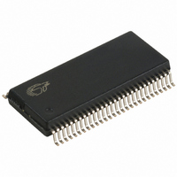
... FIFOADR[1:0] to RD/WR/PKTEND Set-up Time SFA t RD/WR/PKTEND to FIFOADR[1:0] Hold Time FAH 10.0 Ordering Information Table 10-1. Ordering Information Ordering Code CY7C68013-128AC 128 TQFP CY7C68013-100AC 100 TQFP CY7C68013-56PVC 56 SSOP CY7C68013-56LFC 56 QFN CY3681 EZ-USB FX2 Xcelerator Development Kit Document #: 38-08012 Rev. *C Description t t SFA FAH [15] ...
Page 47
... Package Diagrams The FX2 is available in four packages: • 56-pin SSOP • 56-pin QFN • 100-pin TQFP • 128-pin TQFP. Figure 11-1. 56-lead Shrunk Small Outline Package O56 Figure 11-2. 56-lead Quad Flatpack No Lead Package ( mm) LF56 Document #: 38-08012 Rev. *C CY7C68013 51-85062-*C 51-85144-*B Page ...
Page 48
... Figure 11-3. 100-Pin Thin Plastic Quad Flatpack ( 1.4 mm) A101 Document #: 38-08012 Rev. *C CY7C68013 51-85050-*A Page ...
Page 49
... Figure 11-4. 128-Lead Thin Plastic Quad Flatpack ( 1.4 mm) A128 Document #: 38-08012 Rev. *C CY7C68013 51-85101-*B Page ...
Page 50
... Solder Mask Cu Fill Cu Fill 0.013” dia This figure only shows the top three layers of the circuit board: Top Solder, PCB Dielectric, and the Ground Plane Figure 13-2. Plot of the Solder Mask (White Area) CY7C68013 PCB Material Page ...
Page 51
... Semiconductor products in life-support systems application implies that the manufacturer assumes all risk of such use and in doing so indemnifies Cypress Semiconductor against all charges. Figure 13-3. X-ray image of the assembly 2 C system, provided that the system conforms to the I CY7C68013 2 C Standard Specification Page ...
Page 52
... Document History Page Document Title: CY7C68013 EZ-USB FX2™ USB Microcontroller High-speed USB Peripheral Controller Document Number: 38-08012 Issue REV. ECN NO. Date ** 111753 11/15/01 *A 111802 02/20/02 *B 115480 06/26/02 *C 120776 01/06/03 Document #: 38-08012 Rev. *C Orig. of Change Description of Change DSG Change from Spec number: 38-00929 to 38-08012 KKU Update functional changes between revision D part and revision E part ...