20-668-0003 Rabbit Semiconductor, 20-668-0003 Datasheet
20-668-0003
Specifications of 20-668-0003
316-1062
Available stocks


Related parts for 20-668-0003


20-668-0003 Summary of contents
Page 1
... Rabbit 2000 User’s Manual 019–0069 • 070831–P Microprocessor ...
Page 2
... Rabbit 2000 Microprocessor User’s Manual Part Number 019-0069 • 070831–P • Printed in U.S.A. ©2002–2007 Rabbit Semiconductor Inc. • All rights reserved. No part of the contents of this manual may be reproduced or transmitted in any form or by any means without the express written permission of Rabbit Semiconductor. ...
Page 3
... Register to Register Move ..........................................................................................................25 3.3.5 Register Exchanges ....................................................................................................................25 3.3.6 Push and Pop Instructions ..........................................................................................................26 3.3.7 16-bit Arithmetic and Logical Ops ............................................................................................26 3.3.8 Input/Output Instructions ...........................................................................................................29 3.4 How Assembly Language—Tips and Tricks 3.4.1 Zero Clocks ...................................................................................................................31 3.4.2 Exchanges Not Directly Implemented .......................................................................................31 3.4.3 Manipulation of Boolean Variables ...........................................................................................31 3.4.4 Comparisons of Integers ............................................................................................................32 3 ...
Page 4
... Chapter 9. Parallel Ports ............................................................................................................100 9.1 Parallel Port A ............................................................................................................101 9.2 Parallel Port B ............................................................................................................102 9.3 Parallel Port C ............................................................................................................103 9.4 Parallel Port D ............................................................................................................106 9.5 Parallel Port E Chapter 10. I/O Bank Control Registers ........................................................................................41 ............................................................................44 .........................................................................................49 .....................................................................................50 ......................................................................59 ..............................................................................64 .........................................................65 ..........................................................................................72 ......................................................................................76 ..............................................................77 ................................................................................78 .......................................................................................94 ..............................................................................96 ................................................................................97 Rabbit 2000 Microprocessor User’s Manual 109 ...
Page 5
... Slave Port Registers 13.3 Applications and Communications Protocols for Slaves 13.3.1 Slave Applications .................................................................................................................145 13.3.2 Master-Slave Messaging Protocol .........................................................................................146 Chapter 14. Rabbit 2000 Clocks ....................................................................................................150 14.1 Low-Power Design 14.2 Clock Spectrum Spreader Module Chapter 15. AC Timing Specifications 15.1 Memory Access and I/O Read/Write Times ...
Page 6
... Load Immediate Data 18.2 Load & Store to Immediate Address 18.3 8-bit Indexed Load and Store 18.4 16-bit Indexed Loads and Stores 18.5 16-bit Load and Store 20-bit Address 18.6 Register to Register Moves ................................................................................................180 18.7 Exchange Instructions 18.8 Stack Manipulation Instructions 18 ...
Page 7
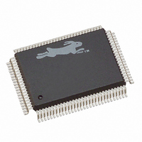
... Software development is accomplished by connecting a simple interface cable from a PC serial port to the Rabbit-based target system. 1.1 Features and Specifications • 100-pin PQFP package. Operating voltage 2 Clock speed to 30 MHz. All specifications are given for both industrial and commercial temperature and voltage ranges. Rabbit microprocessors cost under $10 in moderate quantities. ...
Page 8
... A slave port allows the Rabbit to be used as an intelligent peripheral device slaved to a master processor. The 8-bit slave port has six 8-bit registers, 3 for each direction of communication ...
Page 9
... This is a powerful alternative to sleep modes of operation used by other processors. The current is approximately MHz and 5 V. The current is pro- portional to voltage and clock speed—at 3.3 V and 7.68 MHz the current would be 13 mA, and at 1 MHz the current is reduced to less than 2 mA. Flash memory with auto- matic power down (from AMD) should be used for operation at the lowest power. • ...
Page 10
... Figure 1-1 shows a block diagram of the Rabbit. Figure 1-1. Block Diagram of the Rabbit Microprocessor 4 Rabbit 2000 Microprocessor User’s Manual ...
Page 11
... The Rabbit can be cold booted so unprogrammed flash memory can be soldered in place. • You can write serious software 1,000 or 50,000 lines of C code. The tools are there and they are low in cost. • If you know the Z80 or Z180, you know most of the Rabbit. ...
Page 12
... Rabbit 2000 Microprocessor User’s Manual ...
Page 13
... Some obsolete or redundant Z180 instructions have been dropped to make available efficient 1-byte opcodes for important new instructions. (see “Differences Rabbit vs. Z80/Z180 Instructions” on page 187.) The advantage of this evolutionary approach is that users familiar with the Z80 or Z180 can immediately understand the Rabbit. Existing source code can be assembled or compiled for the Rabbit with minimal changes ...
Page 14
... The processor clock can also be driven by the 32.768 kHz oscillator for very low power opera- tion, in which case the main oscillator can be shut down under software control. 8 Rabbit 2000 Microprocessor User’s Manual ...
Page 15
... Applications include communications signaling, pulse width modulation and driving stepper motors. Chapter 2 Rabbit Design Features Power Clock Speed Voltage (mW) (MHz) 400 6.0 200 3.0 87 1.5 42 0.032 Port Output Timer Clock Current Power (V) ...
Page 16
... The output of four of the timers is used to provide baud clocks for the serial ports. Any of these registers can also cause interrupts and clock the timer-synchronized parallel output ports. Timer B consists of a 10-bit 10 Rabbit Input Register Output Registers Slave Interface Registers Rabbit 2000 Microprocessor User’s Manual CPU ...
Page 17
There are two 10-bit match registers and compar- ators. If the match register matches the counter, a pulse is output. Thus the timer can be programmed to output a pulse at a ...
Page 18
... Programming Port Rabbit Semiconductor publishes a specification for a standard programming port (see Appendix A.1, “The Rabbit Programming Port,”) and provides a converter cable that may be used to connect a PC serial port to the standard programming interface. The interface is implemented using a 10-pin connector with two rows of pins centers. The port is ...
Page 19
... M 3.1 Processor Registers The Rabbit’s registers are nearly identical to those of the Z180 or the Z80. The figure below shows the register layout. The XPC and IP registers are new. The EIR register is the same as the Z80 I register, and is used to point to a table of interrupt vectors for the exter- nally generated interrupts ...
Page 20
... The Rabbit has new instructions that greatly improve communication between the regular and alternate register set. This effectively doubles the number of registers that are easily available for the programmer’s use not intended that the alternate register set be used to provide a separate set of registers for an interrupt routine, and Dynamic C does not sup- port this usage because it uses both registers sets freely ...
Page 21
... The segment register has eight bits and those eight bits are added to the upper four bits of the 16-bit address, creating a 20-bit address. Thus, each separate zone in the 16-bit memory becomes a window to a segment of memory in the 20-bit address space. ...
Page 22
... It may be an extension of 16 10000 XPC segment E000 stack segment D000 data segment 7000 root segment 0000 16-bit address space Rabbit 2000 Microprocessor User’s Manual 10000 0E000 85 93000 0D000 80 8D000 07000 79 80000 07000 00000 20-bit ...
Page 23
... For example 512K x 8 flash mem- ory accessed in the first 512K of the 20-bit address space, then /CS0, /WE0, /OE0 could be enabled in both quadrants. ...
Page 24
... Program code can reside in the root segment or the XPC segment. Program code may also be resident in the data segment. Code can be executed in the stack segment, but this is usu- ally restricted to special situations. Code in the root, meaning any of the segments other 18 Rabbit 2000 Microprocessor User’s Manual ...
Page 25
... XPC segment is called. Functions located in the root have an efficiency advantage because a long call and a long return require 32 clocks to execute, but a short call and a short return require only 20 clocks to execute. The differ- ence is small, but significant for short subroutines. ...
Page 26
... Since the stack has to be moved into the data area important that the number of stacks required be kept to a minimum when using the stack segment to view data. Of course, tasks that don’t need to see the data structures can have their stack located in the stack segment. Another possibility is to have a data structure and a stack located together in the stack segment, and to use a different stack segment for different tasks, each task having its own data area and stack bound to it ...
Page 27
... If only one stack is needed, then it is possible to eliminate the stack segment entirely and place the single stack in the data seg- ment. This option is attractive for systems with only 32K of RAM that don’t need multiple stacks. ...
Page 28
... Three clocks are needed for each data byte written. One additional clock is required if a memory address needs to be computed or an index register is used for addressing. Only a few instructions don’t follow this pattern. An example is mul bit signed two’s complement multiply. mul is a 1-byte op code, but requires 12 clocks to execute. ...
Page 29
... I/O devices. Some Z80 and Z180 instructions have been deleted and are not supported by the Rabbit (see Chapter 19, “Differences Rabbit vs. Z80/Z180 Instructions,”). Most of the deleted instructions are obsolete or are little-used instructions that can be emulated by several Rabbit instructions ...
Page 30
... LD HL',(HL+d) LD (HL+d),HL LD (IX+d),HL ; store HL at address pointed plus -128 to +127 offset LD HL,(IX+d) LD HL',(IX+d) LD (IY+d),HL ; store HL at address pointed plus -128 to +127 offset LD HL,(IY+d) LD HL',(IY+ The only destination for a load is HL Rabbit 2000 Microprocessor User’s Manual HL' ...
Page 31
Register to Register Move Any of the 8-bit registers and L, can be moved to any other 8-bit regis- ter, for example: LD A,c LD d,b LD e,l The alternate 8-bit registers can ...
Page 32
... IX right with carry, 2 bytes, 4 clocks rotate IY right with carry ;Logical Operations AND HL, byte, 2 clocks AND IX, bytes, 4 clocks AND IY,DE OR HL, byte, 2 clocks OR IX, bytes, 4 clocks OR IY, used when the destination regis- ALTD flag Rabbit 2000 Microprocessor User’s Manual and instructions ADD ADC ) may be ALTD ...
Page 33
The instruction is a special instruction designed to help test the HL register. BOOL sets HL to the value non zero, otherwise zero its value is not changed. The flags are set according ...
Page 34
... The multiply instruction can also be used to perform left or right shifts. A left shift of n positions can be accomplished by multiplying by the unsigned number 2^^n. This works for n # 15, and it doesn’t matter if the numbers are signed or unsigned. In order right shift < n < 16), the number should be multiplied by the unsigned number 2^^(16 – ...
Page 35
... I/O devices. In certain conditions where an I/O operation is followed by a special one-byte instruction, a bug in the original Rabbit 2000 chip causes an I/O access to take place instead of a mem- ory access operation. The problem was corrected in revisions A–C of the Rabbit 2000. ...
Page 36
... Dynamic C compiler or in any of the stan- dard libraries. Beginning with the 6.57 release, the Dynamic C compiler and assembler will correct for this anomaly by inserting NOPs 30 between the I/O instruction and a follow- NOP where necessary in generated code. Rabbit 2000 Microprocessor User’s Manual ...
Page 37
... LD IX/IY,HL EX DE, clocks total 3.4.3 Manipulation of Boolean Variables Logical operations involving HL when logical variable with a value 0— this is important for the C language where the least bit of a 16-bit integer is used to repre- sent a logical result Logical operator—invert bit four clocks (also works for ...
Page 38
... The zero flag is set if the numbers are equal. With the SBC instruction the carry cleared is set if the number subtracted is less than or equal to the number it is subtracted from. 8-bit unsigned integers span the range 0–255. 16-bit unsigned integers span the range 0–65535. ...
Page 39
... For signed integers the conventional method to look at the zero flag, the minus flag and the overflow flag. Signed 8-bit integers span the range –128 to +127 (0x80 to 0x7F). Signed 16-bit integers span the range –32768 to + 32767 (0x8000 to 0x7FFF). The sign and zero flag tell which is the larger number after the subtraction unless the overflow is set, in which case the sign flag needs to be inverted in the logic, that is wrong ...
Page 40
... LDIR LDDR tions. Word stores to I/O space can be used to set two I/O registers at adjacent addresses with a single noninterruptable instruction mapped to unsigned integers ; result is -1, else zero 1111... 100... 011... 000... HL--, DE-- Rabbit 2000 Microprocessor User’s Manual ...
Page 41
... LD A,EIR LD EIR,A Interrupts are initiated by hardware devices or by certain 1-byte instructions called reset instructions. RST 10 RST 18 RST 20 RST 28 RST 38 The instructions are similar to those on the Z80 and Z180, but certain ones have been RST removed from the instruction set (00, 08, 30). The less of the processor priority ...
Page 42
... Devices that need extremely fast response to interrupts will use priority level interrupts. Since code that runs at priority level never disables level 2 and level 3 interrupts, these interrupts will take place within about 20 clocks, the length of the longest instruction or longest sensible sequence of privileged instructions followed by an unprivi- leged instruction ...
Page 43
... E. If several lines are to share interrupts with the same port, the individual interrupt requests would normally be or’ed together so that any device can cause an interrupt. If several devices are requesting an interrupt at the same time, only one interrupt results because there will be only one transition of the interrupt request line. To resolve the situation and ...
Page 44
... No interrupt can be allowed between the test of the bit and the setting of the bit as this might allow two different program to both think they own the resource. 38 Rabbit 2000 Microprocessor User’s Manual ...
Page 45
Computed Long Calls and Jumps The instruction to set the XPC is privileged to so that a computed long call or jump can be made. This would be done by the following sequence. LD xpc,a JP (HL) In this ...
Page 46
... Rabbit 2000 Microprocessor User’s Manual ...
Page 47
... Popping registers requires 7–9 clocks. Return from inter- rupt requires 7 clocks. If three registers are saved and restored, and 20 instructions averag- ing 5 clocks are executed, an entire interrupt routine will require about 200 clocks µs with a 20 MHz clock. Given this timing, the following capabilities become possible. ...
Page 48
... Timer B can count as fast sysclk as 10 MHz with a 20 MHz system clock, allowing events to be separated by as little as 100 ns. Timer B and the match registers have 10 bits. Using Timer B, output pulses can be positioned to an accuracy of be used to capture the time at which an external event takes place in conjunction with the external interrupt line ...
Page 49
... A 25%, 50% or 75% duty cycle could operate on a 200 µs period. A 250 µs period would allow duty cycles of 20%, 40%, 60% or 80%. The code for such an interrupt routine might appear as follows ...
Page 50
... The advantage of using open-drain outputs is that if two keys in the same col- umn are depressed, there will not be a fight between a driver driving the line high and another driver driving it low. + o.d. + o.d. Figure 4-2. Using Open-Drain Outputs for Key Scan Rabbit 2000 Microprocessor User’s Manual + ...
Page 51
... The standard programming cable for Dynamic C allows the development platform to reset and cold boot the target, a Rabbit-based microprocessor board. • If the Rabbit is used as a slave processor, the master processor can cold boot it over via the slave port. This means the slave can operate without any nonvolatile memory. Only RAM is required ...
Page 52
... For a detailed description, see Chapter 13 Rabbit Slave Port The slave processor’s slave port is connected to the master processor’s data bus. Commu- nication between the master and the slave takes place via three registers, implemented in the Rabbit, for each direction of communication, for a total of six data registers ...
Page 53
... UART. In this case, a full-duplex transfer can take place, similar to what can be done with a UART. The overhead for such an interrupt-driven trans- fer will be on the order of 100 clocks per byte transferred, assuming a 20-instruction inter- rupt routine. (To keep the interrupt routine to 20 instructions, the interrupt routine needs to be very focused as opposed to general purpose ...
Page 54
... Rabbit 2000 Microprocessor User’s Manual ...
Page 55
... A10 7 /CS0 /SCS, I7, PE7 21 I6, PE6 22 INT1B, I5, PE5 23 INT0B, I4, PE4 24 I3, PE3 25 I2, PE2 26 VSS 27 VDD 28 INT1A, I1, PE1 29 INT0A, I0, PE0 30 Figure 5-1. Package Outline and Pin Assignments Chapter 5 Pin Assignments and Functions F UNCTIONS 80 /WE1 79 A19 78 VDD 77 VSS 76 /OE1 ...
Page 56
... Figure 5-2. Mechanical Dimensions Rabbit PQFP Package Figure 5-3 shows the PC board land pattern for the Rabbit 100-pin PQFP. This land pat- tern is RLP 711A, the registered land pattern for the Rabbit 2000 chip as developed by the Surface Mount Land Patterns Committee and specified in IPC-SM-782A, Surface Mount Design and Land Pattern Standard, IPC, Northbrook, IL, 1999 ...
Page 57
Figure 5-3. PC Board Land Pattern for Rabbit 100-pin PQFP Chapter 5 Pin Assignments and Functions 51 ...
Page 58
... Quartz crystal for main system oscillator. Do not connect if an external clock is used. Address bus. WDT timeout—outputs a pulse when the internal watchdog times out. May also be used to output a 30 µs pulse. Programmable for functions: 1. driven low on first opcode fetch cycle 2 ...
Page 59
... Memory Write Enable 1—connect directly to static memory chip. This pin may be disabled under software control to write protect the chip. I/O Buffer Enable—this signal is driven low during an external I/O cycle and may be used to control 3-state enable on the bus buffer. The purpose is to save power by not driving the I/O address or data lines on every bus cycle ...
Page 60
... On reset these pins are set to inputs and they float. I/O Port B. When used as parallel I/O, PB7 and PB6 are outputs only. PB0–PB5 are inputs only. PB0 and PB1 can be outputs when set up as the clock for the clocked serial ports. On reset, the outputs are set to zero ...
Page 61
... PE1 must also be enabled and similarly for PE4 and PE5. The interrupt is triggered in software on fall, rising or both edges. If both interrupts are enabled, they are or’ed together after edge detection has been performed on each input individually. The port bits must be set up as inputs for the to use them as interrupt request inputs ...
Page 62
... PB1. Clock for serial port B when operating in synchronous mode. Alternate assignment for PB0. Serial inputs and output for serial ports A– D. These are alternate pin assignments for parallel port C. Alternate serial inputs and output for serial ports A and B. These are alternate pin assignments for parallel port D, PD4– ...
Page 63
... I/O space or 8K addresses. Each strobe can be programmed as: chip select, read, write, combined read or write. These are alternate pin assignment for parallel port E, bits 0–7. Each pin may be individually re- assigned from parallel port to strobe functionality. These pins are sampled and an interrupt ...
Page 64
... The user should not attempt a design that uses the chip select or a memory address as a clock or state changing signal without taking this into con- sideration. 58 Address (20 for memory, 16 for I/O) /IOCSn or /CSn /OEn or /IORD and /BUFEN (/BUFEN rd or wr) Data for read ...
Page 65
Description of Pins with Alternate Functions Table 5-2. Pins With Alternate Functions Pin Name Output Function 1. Low on first op code fetch. STATUS (38) 2. Low on interrupt acknowledge SMODE1 (35) SMODE0 (36) 1. Peripheral clock. CLK (1) ...
Page 66
... PE4 (24) /I4 PE3 (25) /I3 PE2 (27) /I2 PE1 (29) /I1 PE0 (30) /I0 60 Input Function Other Function CLKA CLKB RXA RXB RXC RXD ARXA ARXB /SCS (slave chip select). INT1 (input) INT0 (input) INT1 (input) INT0 (input) Rabbit 2000 Microprocessor User’s Manual ...
Page 67
... NOTE: Stresses beyond those listed in Table 5-3 may cause permanent damage. The rat- ings are stress ratings only, and functional operation of the Rabbit 2000 chip at these or any other conditions beyond those indicated in this section is not implied. ...
Page 68
... CMOS Output High Voltage –40°C to +85° Test Conditions Min 5 5 5.0 V, 25° See Table 5-6 OL (sinking 4 See Table 5-6 OH (sourcing Rabbit 2000 Microprocessor User’s Manual Typ Max Units 10 µA µA 10 µA 0 2.4 V 0.2 0.4 V 4.2 V ...
Page 69
... I IL up) I Output Leakage (no pull-up CMOS Input Low Voltage IL V CMOS Input High Voltage IH V CMOS Switching Threshold CMOS Output Low Voltage OL V CMOS Output High Voltage OH Chapter 5 Pin Assignments and Functions = –40°C to +85° Test Conditions Min =3. =3. ...
Page 70
... The maximum DC sinking current for I/O buffers between V 150 mA. ‡ The maximum DC output drive on I/O buffers must be adjusted to take into consideration the current demands made my AC switching out- puts, capacitive loading on switching outputs, and switching voltage. The current ascribed to AC switching is the average current that flows while AC switching is taking place ...
Page 71
... Default Values for all the Peripheral Control Registers The default values for all of the peripheral control registers are shown in Table 6-1. Addi- tional I/O registers were added in the Rabbit 2000 revisions as listed in the table. Refer to Section B.2.1 for more information. ...
Page 72
... I/O Bank 5 Control Register I/O Bank 6 Control Register I/O Bank 7 Control Register Interrupt 0 Control Register Interrupt 1 Control Register Memory Bank 0 Control Register (Rev A–C) Memory Bank 0 Control Register (original chip) MB0CR Memory Bank 1 Control Register Memory Bank 2 Control Register Memory Bank 3 Control Register MMU Instruction/Data Register (controls I & ...
Page 73
Table 6-1. Rabbit Internal I/O Registers (continued) Register Name Port D Data Direction Register Port D Bit 0 Register Port D Bit 1 Register Port D Bit 2 Register Port D Bit 3 Register Port D Bit 4 Register Port ...
Page 74
... Serial Port D Control Register Serial Port A Long Stop Register (Rev A–C) Serial Port B Long Stop Register (Rev A–C) Serial Port C Long Stop Register (Rev A–C) Serial Port D Long Stop Register (Rev A–C) Slave Port Control Register Slave Port Data 0 Register Slave Port Data 1 Register ...
Page 75
Table 6-1. Rabbit Internal I/O Registers (continued) Register Name Timer B Control/Status Register Timer B Control Register Timer B MSB 1 Register Timer B LSB 1 Register Timer B MSB 2 Register Timer B LSB 2 Register Timer B Count ...
Page 76
... Rabbit 2000 Microprocessor User’s Manual ...
Page 77
... One register (GCPU) identifies the CPU, and the other register (GREV) is reserved for revision identification. The CPU identification (GCPU) of all revisions of the Rabbit 2000 microprocessor is the same. Rabbit 2000 revi- sions are differentiated by the value in the GREV register. Refer to Section B.2.2 for more information ...
Page 78
... DISABLE Main Osc Doubler 32 kHz Osc To Watchdog Timer and Time/Date Clock Note: Peripherals cannot be clocked slower than CPU f/2 Clock f/8 Figure 7-1. Clock Distribution Rabbit 2000 Microprocessor User’s Manual ext pin f/2 CLK CPU Peripheral Devices ...
Page 79
Table 7-1. Global Control/Status Register (I/O adr = 0x00) Bit(s) Value 7 reset or watchdog timer timeout since the last read. The watchdog timer timed out. These bits are cleared by a read of this (read only) 01 ...
Page 80
... Table 7-3 lists the recommended values or “settings” for the Global Clock Double Register for various oscillator frequencies. Table 7-3. Recommended Delays Set In GCDR for Clock Doubler Recommended GCDR Value 74 ...
Page 81
... The doubled clock-low time is subject to wide (50%) variation since it depends on process parameters, temperature, and voltage. The times given above are for a supply voltage and a temperature of 25°C. The doubled clock-low time increases by 20% when the voltage is reduced and increases by about 40% when the voltage is reduced further to 3.3 V. ...
Page 82
... This is permissible if nothing, particularly timers and serial ports, depends on the peripheral clock. • If the clock doubler is in use, turn it off, dividing both processor and peripheral by 2. • Divide the processor and/or peripheral clock by 8. • Run code in RAM rather than flash memory. ...
Page 83
Output Pins CLK, STATUS, /WDTOUT, /BUFEN Certain output pins can have alternate assignments as specified in Table 7-4. Table 7-4. Global Output Control Register (GOCR = 0x0E) Bit(s) Value 7:6 00 CLK pin is driven with peripheral clock. 01 ...
Page 84
... The time for this ripple to take place is a few nanoseconds per bit, and certainly should not should not exceed 200 ns for all 8 bits, even when operating at low voltage. The 48 bits are enough bits to count up 272 years at the 32 kHz clock frequency. By con- vention January 1, 1980, is taken as time zero ...
Page 85
... Resets all six bytes of the RTC counter to 0x00 if preceeded by arm command 0x40. Resets all six bytes of the RTC counter to 0x00 and enters byte increment mode—precede this command with 0x40 arm command. This bit combination must be used with every byte increment write to increment clock(s) register corresponding to bit(s) set to "1". ...
Page 86
... The watchdog timer is a 17-bit counter. In normal operation it is driven by the 32.768 kHz clock. When the watchdog timer reaches any of several values corresponding to a delay of from 0. seconds, it “times out.” When it times out, it emits a 1-clock pulse from the watchdog output pin and it resets the processor via an internal circuit. To prevent this tim- eout, the program must “ ...
Page 87
Table 7-9. Watchdog Timer Test Register (WDTTR adr = 0x09) Bit(s) Value Clock the least significant byte of the WDT timer from the peripheral 7:0 0x51 clock. (Intended for chip test and code 0x54 below only.) Clock the most significant ...
Page 88
... Rabbit CPU. Note that the /RESET signal must be held low for three clocks for the proces- sor to begin the reset sequence. There is no facility to tri-state output lines such as the address lines and the memory and I/O control lines. 82 Rabbit 2000 Microprocessor User’s Manual ...
Page 89
... Input/Output PC[7:0] PD[7:0] Input/Output PE[7:0] Input/Output * A low is recognized internally by the processor after a reset † The default state of the I/O ports after the completion of the reset and initializa- tion sequences Chapter 7 Miscellaneous I/O Functions /RESET Low Recognized by CPU Input Low or High Output ...
Page 90
... No interrupts No interrupts No interrupts No interrupts No interrupts No interrupts INT0 {EIR, 0x00} INT1 {EIR, 0x10} {IIR, 0xA0} {IIR, 0xB0} {IIR, 0xC0} {IIR, 0xD0} {IIR, 0xE0} {IIR, 0xF0} {IIR, 0x20} {IIR, 0x30} {IIR, 0x40} {IIR, 0x50} {IIR, 0x70} Rabbit 2000 Microprocessor User’s Manual ...
Page 91
... The interrupt automatically raises the processor’s priority to its own priority. The old processor priority is pushed into the 4- position stack of priorities contained in the IP register. Multiple devices can be requesting interrupts at the same time ...
Page 92
... The problem was corrected in revisions A–C of the Rabbit 2000. (Refer to Appendix B for further information to determine which version of the Rabbit 2000 chip you are using.) If you are working with an original Rabbit 2000 chip, see Technical Note 301, Rabbit 2000 Microprocessor Interrupt Problem. ...
Page 93
... External interrupt Routine #0 (programmed priority could be 3) int2: PUSH IP ; save interrupt priority IPSET 1 ; set to priority really desired (1, 2, etc.) ; insert body of interrupt routine here ; POP IP ; get back entry priority IPRES ; restore interrupted routine’s priority RET ; return from interrupt Chapter 7 Miscellaneous I/O Functions 87 ...
Page 94
... Parallel Ports B and E are used for the Slave Port control signals. Only Slave Port Data Register 0 is used for bootstrap operation, and any writes to the other data registers will be ignored by the processor, and can actually interfere with the bootstrap operation by mask- ing the Write Empty signal. 88 Rabbit 2000 Microprocessor User’s Manual ...
Page 95
... Although the TXA signal is not needed during the first phase of the boot NOTE: procedure, sending the “byte triplets,” two-way communication is required once the cold loader has been loaded. The transfer rate in any bootstrap operation must not be too fast for the processor to exe- cute the instruction stream ...
Page 96
... Rabbit 2000 Microprocessor User’s Manual ...
Page 97
... SEGSIZE register to 0x0DFFF. For exam- ple, if the upper 4 bits of SEGSIZE are 0x0D, then the stack segment will occupy 0x0D000–0x0DFFF, or 4K. If the upper 4 bits of SEGSIZE are greater than or equal to 0x0E, the stack segment vanishes. If these bits are set to zero, the two segments below the stack segment will vanish ...
Page 98
... Every address must belong to one of the possible 4 segments. 2. Each segment has an 8-bit segment register. The 8-bit segment register is added to the upper 4 bits of the 16-bit address to create a 20-bit address. Wraparound occurs if the addition would result in an address that does not fit in 20 bits. ...
Page 99
... Memory Interface Unit The 20-bit memory addresses generated by the memory-mapping unit feed into the mem- ory interface unit. The memory interface unit has a separate write-only control register (see Table 8-3) for each 256K quadrant of the 1M physical memory. This control register specifies how memory access requests to that quadrant are to be dispatched to the memory chips connected to the Rabbit ...
Page 100
... This allows each bank to contain four 256K byte pages, only one of which is available at a time. In revisions A–C of the Rabbit 2000 chip, the reset state of the MB0CR register is set to inhibit /WE0. See Section B.2.6 for more information. ...
Page 101
... Memory Timing Control Register 8.3.3.1 Early Memory Output-Enable Feature The early I/O enable feature was added to the Rabbit 2000C revision to relax the tight tim- ing requirements for memory access when using the clock spectrum spreader. See Section B.2.13 for more information. ...
Page 102
... Dynamic C also supports extended data constants. These are mixed in with the extended code in flash. 96 1024K Variables Stacks Available RAM 512K Extended code Root code and constants 0K Rabbit 2000 Microprocessor User’s Manual ...
Page 103
... The 16-bit PC controls the address of the instruction, usually in the region E000 to FFFF. The advantage of paged access is that most instructions continue to use 16-bit addressing. Only when an out-of-range transfer of control is made does a 20-bit transfer of control need to be made. The beauty of having a 4K minimum step in page alignment while the size of the page that code can be compiled continuously without gaps caused by change of page ...
Page 104
... Memory Figure 8-4. Compilation of Code Segments in Extended Memory 98 View in 8K window each segment Rabbit 2000 Microprocessor User’s Manual FFFF E000 FFFF E000 ...
Page 105
... Port D bits 0–3 have a higher current drive capability. • Port E—All bits of Port E can be configured as I/O strobes. 4 bits of port E can be used as external interrupt inputs. One bit of port E is shared with the slave port chip select. ...
Page 106
... This could be different than the value stored in the output register if the pin is forced to a different state by an external voltage. 100 Mnemonic I/O address PADR 0x30 SPCR 0x24 Bit 5 Bit 4 Bit 3 Bit 2 PA5 PA4 PA3 PA2 Rabbit 2000 Microprocessor User’s Manual R/W Reset R/W xxxxxxxx R/W 0xx00000 Bit 1 Bit 0 PA1 PA0 ...
Page 107
... However still possible to read PB0–PB5 using the Port B data register even when lines PB2–PB7 are used for the slave port also possible to read the signal driving PB6 and PB7 (this signal is on the signaling lines from the slave port logic). ...
Page 108
... I/O address PCDR 0x50 PCFR 0x55 Bit 5 Bit 4 Bit 3 Bit 2 Echo Echo PC5 in PC3 in drive drive x PC4 x PC2 Drive Drive x x TXB TXC Rabbit 2000 Microprocessor User’s Manual R/W Reset R/W x0x0x0x0 W x0x0x0x0 Bit 1 Bit 0 Echo PC1 in drive x PC0 Drive x TXD ...
Page 109
... PDDCR—Parallel port D drive control register. A "1" makes the corresponding pin an open-drain output if that pin is set up for output. Write only. • PDFR—Parallel port D function control register. This port may be used to make port positions 4 and 6 be serial port outputs. Write only. ...
Page 110
... PDCR—Parallel port D control register. This register is used to control the clocking of the upper and lower nibble of the final output register of the port. On reset, bits and 5 are reset to zero. I/O Data perclk/2 Timer A1 Timer B1 Timer B2 perclk/2 Timer A1 Timer B1 Timer B2 Figure 9-1. Parallel Port D Block Diagram ...
Page 111
... PD2 x x PD3 x x PD4 x x PD5 Bits 3, 2 00—clock lower nibble on pclk/2 01—clock on timer A1 x 10—clock on timer B1 11—clock on timer B2 Bit 1 Bit 0 PD1 PD0 out = out = open open drain drain x x dir = dir = out out x PD0 PD1 ...
Page 112
... The output registers are cascaded and timer-controlled, making it possible to generate precise timing pulses. I/O Data perclk/2 Timer A1 Timer B1 Timer B2 perclk/2 Timer A1 Timer B1 Timer B2 Figure 9-2. Parallel Port E Block Diagram 106 /scs PE7 I7 I6 INT1 I5 PE4 INT0 I4 Inputs PE3 I3 I2 INT1 I1 PE0 I0 INT0 Rabbit 2000 Microprocessor User’s Manual ...
Page 113
... The data direction must be set to output for the I/O strobe to work. • PEBxR—These are individual registers to set individual output bits on or off. • PECR—Parallel port E control register. This register is used to control the clocking of the upper and lower nibble of the final output register of the port. On reset, bits and 5 are reset to zero ...
Page 114
... PE2 x x PE3 x x PE4 x x PE5 Bits 3, 2 00—clock lower nibble on pclk/2 01—clock on timer A1 x 10—clock on timer B1 11—clock on timer B2 Rabbit 2000 Microprocessor User’s Manual Bit 1 Bit 0 PE1 PE0 alt /I1 alt /I0 dir = dir = out out x PE0 PE1 Bits 1, 0 ...
Page 115
... Wait state code 00—chip select 11-1 01—read strobe 10-3 10—write strobe 01-7 11—or of read and 00-15 write strobe * Total number of external I/O read/write wait states, including the one wait state that is always present. Chapter 10 I/O Bank Control Registers C ANK ...
Page 116
... Pin A[15:13] Range PE0 000 0x0000–0x1FFF PE1 001 0x2000–0x3FFF PE2 010 0x4000–0x5FFF PE3 011 0x6000–0x7FFF PE4 100 0x8000–0x9FFF PE5 101 0xA000–0xBFFF PE6 110 0xC000–0xDFFF PE7 111 0xE000–0xFFFF Rabbit 2000 Microprocessor User’s Manual ...
Page 117
... There are two timers—Timer A and Timer B. Timer A is intended mainly for generating the baud clock for the serial ports, a periodic clock for clocking parallel ports D and E, or for generating periodic interrupts. Timer B can be used for the same functions, but it can- not generate the baud clock ...
Page 118
... Timers A4, A5, A6 and A7 always provide the baud clock for serial ports and D respectively. Except for very low baud rates, clock A1 does not need to be used to prescale the input clock for timers A4–A7. For example, if the system clock is 11.0592 MHz, and if the timer A4 divides by 144, an asynchronous baud rate of 2400 bps can be achieved in one step ...
Page 119
... Writing to these bits enables the interrupts for the corresponding timer. Bit 0—Write, set to a "1" to enable the clock (perclk/2) for Timer A, set to "zero" to dis- able the clock (perclk/2 in Figure 11-1). Bits 1 and 4–7 are written (write only) to enable the interrupt for the corresponding timer ...
Page 120
... A1 and the reload register should be set to 255. This will cause counting slow as possible and consume minimum power. Timer A has five separate subtimer units, A1 and A4–A5, that are also referred to as timers. Most likely serial port is going to be used and a timer is needed to provide the baud clock, that timer will be set driven directly from the clock, and the interrupt asso- ciated with that timer will be disabled ...
Page 121
... If another value is written to the same register, it will stay in the holding register. Once a match occurs, the value in the TBLxR match register is flagged as “invalid.” At that time value is in the holding register, it will get transferred to the match register, assuming that the Timer B clock is running ...
Page 122
... Bits 7:4 00—Counter clocked by perclk/2 Not used 01—Counter clocked by output of timer A1 1x—Timer clocked by perclk/2 divided by 8 The MSB x registers for Timer B (TBM1R/TBM2R) are laid out as shown in Table 11-7. Table 11-7. Timer B MSB x Register (TBM1R/TBM2R = 0x0B2/0x0B4) Bits 7:6 Two most significant bits of timer match preload register ...
Page 123
Using Timer B Normally the prescaler is set to divide appropriate to the problem. For example, if the clock is 22.1184 MHz, then 11.0592 MHz. A Timer B clock rate of 11.0592 MHz will cause a complete cycle of ...
Page 124
... MHz, the counter can count as fast as 10 MHz. The uncertainty in a pulse width measure- ment can be nearly as low as 38 clocks (2 x 19), or about 2 µs for a 20 MHz system clock. Timer B can be used to change a parallel port output register at a particular specified time in the future ...
Page 125
... Two features related to asynchronous and clocked serial communication were added to the Rabbit 2000 serial port hardware in revisions A–C to improve and simplify asynchronous serial and clocked serial communication. See Section B.2.3 for more information. The Rabbit has four on-chip serial ports designated and D. All the ports can perform asynchronous serial communications at high baud rates ...
Page 126
... Timers A4–A7 supply the input clock for Serial Ports A–D. These timers can divide the frequency by any number from 1 to 256 (see Chapter 11). The input frequency to the timers can be selected in different ways described in the documentation for the timers. One choice is the peripheral clock divided by 2— ...
Page 127
... Bit 5—This bit is set if the receiver is overrun. This happens if the shift register and the data reg- ister are full and a start bit is detected. This bit is cleared when the receiver data register is read. ...
Page 128
... Port C and Port D serial outputs (see Section 9.3, “Parallel Port C” and Section 9.4, “Parallel Port D” for more details). Bits 3,2—This sets the mode of operation. Modes 10 and 11 apply only to Ports A and B. Bits 1,0—These bits enable interrupts and set the interrupt priority. ...
Page 129
Serial Port Interrupt A common interrupt vector is used for the receive and transmit interrupts. There is a sepa- rate interrupt request flip-flop for the receiver and transmitter. If either of these flip-flops is set, a serial port interrupt ...
Page 130
... Since it has no more data, it clears the interrupt request by storing to the status register. At this point the routine should check if the shift register is empty; normally it won’t be is, because the interrupt was answered late, the interrupt routine should do any final cleanup and store to the status register again in case the shift register became empty after the pending interrupt is cleared ...
Page 131
... Clocked Serial Ports See Section B.2.3 for more information for more information about a new feature added to revisions A–C to better support full-duplex communication. Ports A and B can operate in clocked mode. The data line and clock line are driven as shown in Figure 12-4. The data and clock are provided as 8-bit bursts. The transmit shift register advances on the falling edge of the clock ...
Page 132
... When the shift register is idle and the receiver provides a clock burst, the data bits are transferred to the shift register and are shifted out. Once the transfer is 126 Pin Function Serial Clock Data Transmit Data Receive Rabbit 2000 Microprocessor User’s Manual ...
Page 133
... For example, if the baud rate is 400,000 bps, then up to 50,000 bytes per sec- ond could be transmitted byte every 20 µs. No data will be lost if the transmitter can answer its interrupts within 20 µs. There will be no slow down if the receiver can answer its interrupt within 1/2 clock or 1.25 µ ...
Page 134
... Figure 12-6. Synchronous Serial Data Transmit Timing with External Clock 128 BIT 1 BIT 2 BIT 3 BIT 4 BIT 1 BIT 2 BIT 3 BIT may take anywhere from clock cycles for the exter- perclk Rabbit 2000 Microprocessor User’s Manual MSB BIT 5 BIT 6 BIT 5 BIT 6 MSB ) before data can be perclk , the external serial clock, and ...
Page 135
Figure 12-7 shows the timing relationship among data receive. Note that RxA is sampled by the rising edge of perclk CLKA (Ext.) RxA Figure 12-7. Synchronous Serial Data Receive Timing with External Clock When clocking the Rabbit externally, the maximum ...
Page 136
... At 115,200 bps, the highest speed serial port, the interrupts must be serviced in 10 baud times µs, in order not to lose the received characters. If all four serial ports were operat- ing at this receive speed, it would be necessary to service the interrupt in less than 21.5 µs to assure no lost characters ...
Page 137
... RS-485 driver and possibly enable the receiver. 12.7.2 Transmitting Dummy Characters It may be desired to operate the serial transmitter without actually sending any data. “Dummy” characters are transmitted to pass time or to measure time. The output of the transmitter may be disconnected from the transmitter output pin by manip- ulating the control registers for parallel port which are used as output pins ...
Page 138
... Some systems may require two stop bits. In some cases, it may be necessary to send a par- ity bit. Certain systems, such as some 8051-based multidrop communications systems, use a 9th data bit to mark the start of a message frame. The Rabbit 2000 can receive parity or message formats that contain a 9th bit without problem. Transmitting messages with par- ity or messages that always contain a 9th bit is also possible ...
Page 139
... If the first stop bit is missing treated as a 9th (or 8th) bit low and will be received as a 9-bit (8-bit) character. Sending a 9th bit or an extra stop bit is easier with revisions A–C of the Rabbit 2000 chip, which have a long stop register as described in Section B.2.3. It was more difficult to transmit an extra stop bit or a parity bit of value " ...
Page 140
... Requests from the network master to one of its slaves consist of a frame of bytes—the first byte has the 9th bit set to "1" (as the signal is observed at the Tx pin of the processor) and the following bytes have the 9th bit set to "0." ...
Page 141
... This scheme reduces the overhead associated with messages directed to other slaves, but it does not really help with the worst-case load. In most cases, the worst-case compute load is the governing factor for embedded systems ...
Page 142
... Rabbit 2000 Microprocessor User’s Manual ...
Page 143
When a Rabbit microprocessor is configured as a slave, parallel port A and certain other data lines are used as communication lines between the slave and the master. The slave unit is a Rabbit configured as a slave. The master ...
Page 144
... The same names are used for different registers since it is usually clear from the context which register is meant necessary to distinguish between registers, we will refer to the registers as “SPD0R writable by the slave” or “SPD0R writable by the master.” ...
Page 145
The registers appear to be internal I/O registers to the slave. To the master, at least for a Rabbit master, the registers appear to be external I/O registers. The figure below shows the sequence of events when the master reads/writes ...
Page 146
... SD Setup Time Th(SD) SD Hold Time Tsu(SRD – SWR) /SRD High to /SWR Low Setup Time The two SPD0R registers have special functionality not shared by the other data registers. If the master writes to SPD0R, an inbound interrupt flip-flop is set. If slave port interrupts are enabled, the slave processor will take a slave port interrupt. If the slave writes to the other SPD0R register, the slave attention line (/SLAVEATTN, pin 100) is asserted (driven low) by the slave processor ...
Page 147
Master writes SPD0R Slave writes status register Slave writes SPD0R Master writes status register Figure 13-3. Slave Port Handshaking and Interrupts Figure 13-4 shows a sample connection of two slave Rabbits to a master Rabbit. The mas- ter drives the ...
Page 148
... If a Rabbit is used as a master, this line is normally connected to the global I/O read strobe /IORD. • /SWR—Input. If /SCS is also low, this line causes the data bits on the data bus to be clocked into the register selected by the address lines on the rising edge of /SWR or /SCS, whichever rises first ...
Page 149
... Figure 13-4 is under the program control of the master. If the master is reset, the slave will also be reset because the master’s drive of the reset line will be lost on reset and the pull- down resistor will pull the slaves’ resets low. This may be undesirable because it forces the slave to crash if the master crashes and has a watchdog timeout ...
Page 150
... The functionality of the bits is as follows: Bit 7—If set to "0," the cold-boot feature will be enabled. Normally this bit is set to a "1" after the cold boot is complete. The cold boot for the slave port is enabled automatically if (SMODE1, SMODE0) lines are set to (0,1) after the reset ends. This features disables the normal operation of the processor and causes commands to be accepted via the slave port register SPD0R ...
Page 151
... Traditional servo system solutions may be overly expensive or not work very well because of system nonlinearities. The basic communications model for a motion controller is for the master to send short messages—positioning com- mands—to the slave. The slave acknowledges execution of the commands and reports exception conditions. • ...
Page 152
... A typical slave system consists of a Rabbit microprocessor and a RAM memory con- nected to it. The clock can be provided either by connecting a crystal, or crystals to the slave or by providing an external clock, which could be the master’s clock. The reset line of the slave would normally be driven by the master. At system startup time the master resets the slave and cold boots it via the slave port ...
Page 153
As a simple example, suppose that the slave used as a four-port UART. It has the capability to send or receive characters on any of its four serial ports. Leaving aside the question of setup for parameters, ...
Page 154
... Rabbit 2000 Microprocessor User’s Manual ...
Page 155
... The Rabbit 2000 has two built-in oscillators. The 32.768 kHz clock oscillator is needed for the battery-backable clock, the watchdog timer, and the cold-boot function. The main oscillator provides the run-time clock for the microprocessor. Figure 14-1 shows these oscillator circuits Figure 14-1. Rabbit 2000 Oscillator Circuits The 32 ...
Page 156
... Clock Spectrum Spreader Module The clock spectrum spreader is a feature that was introduced on the Rabbit 3000 and migrated to revisions B and C of the Rabbit 2000. The clock spectrum spreader is very effective for reducing EMI and radiated emissions because it will reduce all sources of EMI above 100 MHz that are related to the clock by about 15 dB ...
Page 157
... AC T The Rabbit 2000 processor may be operated at voltages between 2.5 V and 5.5 V, and at temperatures from –40°C to +85°C with use possible use over the range -55°C to +120°C. Most users will operate the Rabbit at either 5 3.3 V. The most computation per watt is obtained at approximately 3 ...
Page 158
... These clock speeds are usually multiples of 1.8432 MHz to ensure that baud rates of 57,600 bps, 19,200 bps, and less will be available. Multiples of 3.6862 MHz ensure that baud rates of 115,200 bps, 38,400 bps, and less will be available. Multiples of 1.2288 MHz ensure that baud rates of 38,400 bps and less will be available. The standard Rabbit BIOS will accept any clock speed that is a multiple of 0 ...
Page 159
... Figure 15-1. Rabbit 2000 Typical Maximum Operating Frequency versus Temperature and 3.3 V 50.00 45.00 40.00 35.00 30.00 25.00 20.00 15.00 10.00 5.00 0.00 2 Figure 15-2. Rabbit 2000 Typical Maximum Operating Frequency Chapter 15 AC Timing Specifications Temperature (° Voltage (V) versus Voltage at 25°C 5 ...
Page 160
... The operating power is also proportional to the clock speed. Higher temperatures reduce the maximum operating speed by approximately 1% for each 5°C. In addition, higher operating speeds increase the die temperature because of the heat generated and therefore slightly compound the adverse effects of higher temperature. 154 Rabbit 2000 Microprocessor User’s Manual ...
Page 161
... 3 3.3 V 127 @ 5 V/ 120 @ 5 V/ 123 @ 3.3 V 114 @ 3.3 V 197 @ 5 V/ 190 @ 5 V/ 193 @ 3.3 V 184 @ 3.3 V 172 @ 5 V 165 @ 5 V/ 168 @ 3.3 V 159 @ 3.3 V 162 @ 2.5 V(min) 150 @ 2.5 V(min) 263 @ 5 V/ 256 @ 5 V/ 259 @ 3 ...
Page 162
... The measurements were taken at the 50% points under the following conditions. • -40°C to 85° 5.0 V ±10% • Internal clock to nonloaded CLK pin delay ≤ 85°C/4.5 V The following memory write time delays were measured. Table 15-4. Memory Write Time Delays Time Delay ...
Page 163
Figure 15-3. Memory Read and Write Cycles Notice that the data times are different, depending on whether data are being read or writ- ten. T for data read specifies how long the data must remain valid following the rising hold ...
Page 164
... The measurements were taken at the 50% points under the following conditions. • -40°C to 85° 5.0 V ±10% • Internal clock to nonloaded CLK pin delay ≤ 85°C/4.5 V The following I/O write time delays were measured. Table 15-6. I/O Write Time Delays Time Delay ...
Page 165
... I/O bus cycles have an automatic wait state and thus require 3 clocks plus any extra wait states specified. Figure 15-4. I/O Read and Write Cycles—No Extra Wait States Chapter 15 AC Timing Specifications 159 ...
Page 166
... Figure 15-5 shows the effect of adding an extra wait state to the memory read/write cycles. The effects are similar for the I/O bus read/write cycles. Figure 15-5. Memory Read and Write with Wait States 160 Rabbit 2000 Microprocessor User’s Manual ...
Page 167
... Data read setup time setup T Data read hold time hold Time from CPU clock rising T adr edge to address valid Data write hold time from /WEx T hold or /IOWR Chapter 15 AC Timing Specifications Value Max Min Min Max Min. ½ CPU clock cycle 161 ...
Page 168
... The current consumed by memory and other devices included in the system, including pullup resistors, outputs driving a load, and floating inputs, must be added to the figures in Table 15-8. 162 Voltage Current (V) (mA) 5 109 3.3 36 3.3 19 3.3 11 3.3 6 3.3 4.2 3.3 3.14 5 0.280 4 0.173 3.3 0.113 2.7 0.072 Rabbit 2000 Microprocessor User’s Manual 2 (2) ...
Page 169
The 32.768 kHz clock oscillator and the associated real-time clock consume approxi- mately 23 µ (At 2.25 V, when backed by a battery, the current consumption is approximately 11 µA.) The (typical) current consumed when the main ...
Page 170
... Rabbit 2000 Microprocessor User’s Manual ...
Page 171
... System startup: including setup of memory, wait states and clock speed. • Writing to flash. Writes to the primary code memory require turning off interrupts for so. To protect the System Identification Block (see the Rabbit 2000 Designer’s Handbook for more information on the System ID Block), the flash driver will not write to that block ...
Page 172
... The Rabbit 2000 Designer’s Handbook has a chapter on the Rabbit BIOS with more details. 16.2 Virtual Driver The Virtual Driver is compiled with the user’s application. It includes support for the fol- lowing services. • Hitting the hardware watchdog timer. • Decrementing software watchdog timers. ...
Page 173
... The Virtual Driver’s periodic interrupt hits the hardware watchdog timer with a 2 second time-out. If the periodic interrupt stops working, then the watchdog will time out after 2 seconds. The Virtual Driver provides a number of additional “ ...
Page 174
... Rabbit 2000 Microprocessor User’s Manual ...
Page 175
... Only about 3 instructions could be executed between ticks. A different set of rules applies in the ultra slow or “sleepy” mode. The Rabbit 2000 auto- matically disables periodic interrupts when the clock mode is switched to 32 kHz or one of the multiples of 32 kHz. This means that the periodic-interrupt hardware does not function when running at any of these 32 kHz clock speeds simply because there are not enough clock cycles available to service the interrupt ...
Page 176
... Dynamic C functions are available to read and write I/O registers. These functions are pro- vided for convenience. For speed, assembly code is recommended. For a complete description of the functions noted in this section, refer to the Dynamic C User’s Manual or from the menu in Dynamic C, access the Help options ...
Page 177
... As an example, consider the parallel port D data direction register (PDDDR). This register is write only, and it contains 8 bits corresponding to the 8 I/O pins of parallel port bit in this register is a “1,” the corresponding port pin is an output, otherwise input easy to imagine a situation where different parts of the application, such as an inter- rupt routine and a background routine, need charge of different bits in the PDDDR register ...
Page 178
... Shadow register are not needed for many of the registers that can be written to. In some cases, writing to registers is used as a handy way of changing a peripheral’s state, and the data bits written are ignored. For example, a write to the status register in the Rabbit serial ...
Page 179
... SEC_TIMER when the Virtual Driver starts, and updated every second by the periodic interrupt. It may be read or written directly by the user’s programs. Since same oscillator as the real-time clock there is no relative gain or loss of time between the two. A millisecond timer variable, Two utility routines are provided that can be used to convert times between the traditional format (10-Jan-2000 17:34:12) and the seconds since 1-Jan-1980 format ...
Page 180
... Rabbit 2000 Microprocessor User’s Manual ...
Page 181
... Summary All bugs related to instructions have been fixed in revisions A–C of the Rabbit 2000 chip. See Appendix B for more information. Detailed information on instructions in provided in this chapter. “Load Immediate Data” on page 178 “8-bit Indexed Load and Store” on page 178 “16-bit Indexed Loads and Stores” on page 178 “ ...
Page 182
... The L/V (logical/overflow) flag serves a dual purpose— L/V is set to 1 for logical operations if any of the four most significant bits of the result are 1, and L/V is reset all four of the most significant bits of the result are 0. 176 Description Description Flag Register Key ...
Page 183
... Word register select Word register select Logical zero if all four of the most significant bits of the result are 0. † Logical one if any of the four most significant bits of the result are 1. Chapter 18 Rabbit Instructions Meaning 001 = bit 1, 011 = bit 3, 101 = bit 5, 111 = bit 7 ...
Page 184
... (DE (HL (HL (HL (IX+ (IX+ (IX+ (IY+ (Iy+ (IY+ Operation (HL+ (HL+d+ (HL+d (HL+d+ (SP+ (SP+n+ (SP+n) = IXL; (SP+n+1) = IXH - - - - (SP+n) = IYL; (SP+n+1) = IYH - - - - L = (SP+n (SP+n+ IXL = (SP+n); IXH = (SP+n+ IYL = (SP+n); IYH = (SP+n+ (IX+ (IX+d+ (IX+d (IX+d+ (IY+ (IY+d+ (IY+d (IY+d+1) Rabbit 2000 Microprocessor User’s Manual ...
Page 185
... Load and Store 20-bit Address Instruction clk A LDP (HL),HL 12 LDP (IX),HL 12 LDP (IY),HL 12 LDP HL,(HL) 10 LDP HL,(IX) 10 LDP HL,(IY) 10 LDP (mn),HL 15 LDP (mn),IX 15 LDP (mn),IY 15 LDP HL,(mn) 13 LDP IX,(mn) 13 LDP IY,(mn) 13 Note that the LDP instructions wrap around on a 64K page boundary. Since the LDP instruc- tion operates on two-byte values, the second byte will wrap around and be written at the start of the page if you try to read or write across a page boundary ...
Page 186
... IP = (SP SP IXL = (SP); IXH = (SP+1 SP IYL = (SP); IYH = (SP+1 SP zzl = (SP); zzh = (SP+1); SP=SP+2 -- zz= BC,DE,HL, (SP- (SP-1) = IXH; (SP-2) = IXL SP (SP-1) = IYH; (SP-2) = IYL SP (SP-1) = zzh; (SP-2) = zzl; SP=SP-2 --zz= BC,DE,HL, Operation * * DE, HL DE, IX, SP Rabbit 2000 Microprocessor User’s Manual ss=BC, -- xx=BC, ...
Page 187
ADD IY, ADD SP AND HL, AND IX, AND IY, BOOL BOOL BOOL DEC IX 4 DEC IY 4 DEC ss ...
Page 188
... Operation (HL) = (HL (IX+d) = (IX+ (IY+d) = (IY+ (HL) = (HL (IX+d) = (IX+ (IY+d) = (IY+ Rabbit 2000 Microprocessor User’s Manual ...
Page 189
Fast A register Operations Instruction clk A CPL 2 r NEG 4 fr RLA 2 fr RLCA 2 fr RRA 2 fr RRCA 2 fr 18.14 8-bit Shifts and Rotates RL, RLA C RLC, RLCA C RR, RRA ...
Page 190
... (HL) = {0,(HL)[7,1]}; CY = (HL)[ (IX+d) = {0,(IX+d)[7,1]}; CY = (IX+d)[ (IY+d) = {0,(IY+d)[7,1]}; CY = (IY+d)[ {0,r[7,1]}; Operation - - - - alternate register destinatIn for next Instruction - - - - I/O external prefix - - - - I/O internal prefix Operation (DE) = (HL BC- DE repeat (DE) = (HL BC- DE repeat: Rabbit 2000 Microprocessor User’s Manual ...
Page 191
... XPC; (SP-2) = PCH; (SP-3) = PCL mn (SP- XPC=xpc PCL = (SP); PCH = (SP+1); XPC = (SP+2 PCL = (SP); PCH = (SP+1 SP {f} PCL = (SP); PCH = (SP+1 SP (SP); PCL = (SP+1); PCH = (SP+2 (SP-1) = PCH; (SP-2) = PCL {R,v) v=10,18,20,28,38 only Operation - - - * {IP[5:0], 00 {IP[5:0], 01 {IP[5:0], 10 {IP[5:0], 11 {IP[1:0], IP[7:2 EIR * * - - A = IIR - - - - ...
Page 192
... BIT B,(HL) SET B,(HL) JP z,ihaveit ; here I don’t have it The instruction has no effect on the flags. Since no interrupt takes place after the SET instruction, if the flag is zero that means that the semaphore was not set when tested by the bit instruction and that the set instruction has set the semaphore ...
Page 193
D IFFERENCES The Rabbit is highly code compatible with the Z80 and Z180, and it is easy to port non I/O dependent code. The main areas of incompatibility are instructions that are concerned with I/O or particular hardware implementations. ...
Page 194
... The following Z80/Z180 instructions have been dropped and are not supported. Alterna- tive Rabbit instructions are provided. Z80/Z180 Instructions Dropped CALL CC,ADR TST R ((HL),n) 188 Rabbit Instructions to Use JR (JP) ncc,xxx ; reverse condition CALL ADR xxx: PUSH DE PUSH AF AND r ((HL), n) POP DE ; get A,d POP DE Rabbit 2000 Microprocessor User’s Manual ...
Page 195
... The L/V (logical/overflow) flag serves a dual purpose— L/V is set to 1 for logical operations if any of the four most significant bits of the result are 1, and L/V is reset all four of the most significant bits of the result are 0. Chapter 20 Instructions in Alphabetical Order With Binary Encoding A LPHABETICAL W ...
Page 196
... Bit select: 000 = bit 0, 010 = bit 100 = bit 4, 110 = bit 6, Condition code select NZ NC, 7-bit (signed) displacement. Expressed in two’s complement Word register select destination Word register select alternate BC DE HL' dd' 8-bit (signed) displacement added to PC Condition code select: 000 = NZ (non zero), ...
Page 197
... DEC IY 11111101 DEC r 00-r-101 DEC ss 00ss1011 ss= 00-BC, 01-DE, 10-HL, 11-SP DJNZ j 00010000 EX (SP),HL 11101101 EX (SP),IX 11011101 EX (SP),IY 11111101 Chapter 20 Instructions in Alphabetical Order With Binary Encoding Byte 2 Byte 3 Byte 4 10001110 ----d--- 10001110 ----d--- ----n--- 01ss1010 10000110 ----d--- 10000110 ----d--- ----n--- 00xx1001 00yy1001 ----d--- 10100110 ----d--- 10100110 ----d--- ...
Page 198
... Rabbit 2000 Microprocessor User’s Manual clk ...
Page 199
... LDIR 11101101 LDP (HL),HL 11101101 LDP (IX),HL 11011101 LDP (IY),HL 11111101 LDP (mn),HL 11101101 LDP (mn),IX 11011101 LDP (mn),IY 11111101 Chapter 20 Instructions in Alphabetical Order With Binary Encoding Byte 2 Byte 3 Byte 4 ----n--- ----m--- 01010111 01011111 01110111 01dd1011 ----n--- ----m--- 01dd1001 01dd0001 ----n--- ----m--- ... ... ...
Page 200
... Rabbit 2000 Microprocessor User’s Manual clk ...