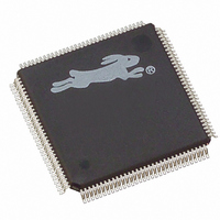
20-668-0011 Rabbit Semiconductor, 20-668-0011 Datasheet - Page 253

20-668-0011
Manufacturer Part Number
20-668-0011
Description
IC MPU RABIT3000A 55.5MHZ128LQFP
Manufacturer
Rabbit Semiconductor
Datasheet
1.20-668-0011.pdf
(312 pages)
Specifications of 20-668-0011
Processor Type
Rabbit 3000 8-Bit
Speed
55.5MHz
Voltage
2.5V, 2.7V, 3V, 3.3V
Mounting Type
Surface Mount
Package / Case
128-LQFP
Data Bus Width
8 bit
Maximum Clock Frequency
55.5 MHz
Operating Supply Voltage
1.8 V to 3.6 V
Maximum Operating Temperature
+ 85 C
Mounting Style
SMD/SMT
Minimum Operating Temperature
- 55 C
Number Of Programmable I/os
56
Lead Free Status / RoHS Status
Lead free / RoHS Compliant
Features
-
Lead Free Status / Rohs Status
Lead free / RoHS Compliant
Other names
316-1061
Available stocks
Company
Part Number
Manufacturer
Quantity
Price
Company:
Part Number:
20-668-0011
Manufacturer:
Rabbit Semiconductor
Quantity:
10 000
- Current page: 253 of 312
- Download datasheet (2Mb)
All important signals on the Rabbit 3000 are output-synchronized with the internal clock.
The internal clock is closely synchronized with the external clock, which is available on
the CLK pin. The delay in signal output depends on the capacitive load on the output lines.
In the case of the address lines, which are critically important for establishing memory
access time requirements, the capacitive loading is usually in the range of 25–100 pF, and
the load is due to the input capacitance of the memory devices and PC trace capacitance.
Delays are expressed from the waveform midpoint in keeping with the convention used by
memory manufacturers.
Table 27-9 lists the delays in gross memory access time for several values of V
When the spectrum spreader is enabled with the clock doubler, every other clock cycle is
shortened or lengthened by a maximum amount given in the table above. The shortening
takes place by shortening the high part of the clock. If the doubler is not enabled, then
every clock is shortened during the low part of the clock period. The maximum shortening
for a pair of clocks combined is shown in the table.
The gross memory access time is 2T, where T is the clock period. To calculate the actual
memory access time, subtract the clock to address output time, the data in setup time, and
the clock period shortening due to the clock spectrum spreader from 2T.
Example Memory Access Time Calculation
• clock = 29.49 MHz, so T = 34 ns
• operating voltage is 3.3 V
• bus loading is 60 pF
• clock to address output delay = 8 ns (see Table 27-9)
• data setup time = 1 ns
• spectrum spreader is on in 1 ns mode, resulting in a loss of 3 ns worst-case (see
Chapter 27 Specifications
Table 27-9)
V
(V)
3.3
2.7
2.5
1.8
DD
30 pF 60 pF 90 pF
Clock to Address
18
6
7
8
Output Delay
Table 27-9. Preliminary Data and Clock Delays
(ns)
10
11
24
8
(V
13
15
33
11
DD
±10%, Temp. -40
Data Setup
Time Delay
(ns)
1.5
1.5
1
3
0.5 ns setting
no dbl / dbl
°
3.5/5.5
C to 85
3/4.5
8/12
4/6
Spectrum Spreader Delay
°
C)
Worst-Case
1 ns setting
no dbl / dbl
5.5/11
11/22
4.5/9
(ns)
6/12
2 ns setting
no dbl / dbl
DD
3.3
2.7
2.5
1.8
.
243
Related parts for 20-668-0011
Image
Part Number
Description
Manufacturer
Datasheet
Request
R

Part Number:
Description:
IC CPU RABBIT2000 30MHZ 100PQFP
Manufacturer:
Rabbit Semiconductor
Datasheet:

Part Number:
Description:
IC CPU RABBIT4000 128-LQFP
Manufacturer:
Rabbit Semiconductor
Datasheet:

Part Number:
Description:
Microprocessors - MPU Rabbit 3000 TFBGA Microprocessor
Manufacturer:
Rabbit Semiconductor

Part Number:
Description:
Microprocessors - MPU Rabbit 4000 LQFP Microprocessor
Manufacturer:
Rabbit Semiconductor

Part Number:
Description:
IC, I/O EXPANDER, 8BIT, 40MHZ, TQFP-64
Manufacturer:
Rabbit Semiconductor

Part Number:
Description:
SCRs 1.5A 200uA 400V Sensing
Manufacturer:
Littelfuse Inc
Datasheet:

Part Number:
Description:
CARD 6-RELAY SMARTSTAR SR9500
Manufacturer:
Rabbit Semiconductor
Datasheet:

Part Number:
Description:
WIRE-BOARD CONN RECEPTACLE, 6POS, 3.96MM
Manufacturer:
TE Connectivity
Datasheet:

Part Number:
Description:
ADAPTER 20 PIN .420" PLUGS(6PCS)
Manufacturer:
Logical Systems Inc.
Datasheet:

Part Number:
Description:
CONN BARRIER BLOCK .438" 20 POS
Manufacturer:
Cinch Connectors
Datasheet:

Part Number:
Description:
20 MODII 2PC HDR DR SHRD, ROHS
Manufacturer:
TE Connectivity
Datasheet:

Part Number:
Description:
WIRE-BOARD CONN RECEPTACLE, 6POS, 3.96MM
Manufacturer:
TE Connectivity
Datasheet:


