Z8018006PSG Zilog, Z8018006PSG Datasheet
Z8018006PSG
Specifications of Z8018006PSG
Q2456016
Z8018006PSG
Available stocks


Related parts for Z8018006PSG


Z8018006PSG Summary of contents
Page 1
... Z80180 Microprocessor Unit Product Specification PS014004-1106 PS014004-1106 ZiLOG Worldwide Headquarters • 532 Race Street • San Jose, CA 95126 Telephone: 408.558.8500 • Fax: 408.558.8300 • www.zilog.com ...
Page 2
... San Jose, CA 95126-3432 Telephone: 408.558.8500 Fax: 408.558.8300 www.zilog.com ZiLOG is a registered trademark of ZiLOG Inc. in the United States and in other countries. All other products and/or service names mentioned herein may be trademarks of the companies with which they are associated. Document Disclaimer ©2006 by ZiLOG, Inc. All rights reserved. Information in this publication concerning the devices, applications, or technology described is intended to suggest possible uses and may be superseded ...
Page 3
Revision History Each instance in the following table reflects a change to this document from its previous revision. To see more detail, click the appropriate link in the table below. Revision Date Level Description November 04 Updated DC Characteristics table ...
Page 4
PS014004-1106 Microprocessor Unit iv ...
Page 5
Table of Contents Overview . . . . . . . . . . . . . . . . . . . . . . . . . . . . . . . . . . . . ...
Page 6
DMA Source Address Register Channel DMA Source Address Register, Channel ...
Page 7
... The Z80180 is an 8-bit MPU which provides the benefits of reduced system costs and also provides full backward compatibility with existing ZiLOG Z80 devices. Reduced system costs are obtained by incorporating several key system functions on-chip with the CPU. These key functions include I/O devices such as DMA, UART, and timer PS014004-1106 ™ ...
Page 8
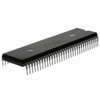
Also included on-chip are wait-state generators, a clock oscillator, and an interrupt controller. ™ The Z80180 is housed in 80-pin QFP, 68-pin PLCC, and 64-pin DIP packages. Note: All signals with an overline are active Low. For example, B/W, ...
Page 9
Pin Configuration V SS XTAL EXTAL WAIT BUSACK BUSREQ RESET NMI INT0 INT1 INT2 A10 A11 A12 A13 A14 A15 A16 A17 A18 V CC Figure 2. Z80180 64-Pin ...
Page 10
Z80180 68-Pin PLCC Pin Configuration 9 INT0 10 INT1 INT2 A10 A11 26 27 Figure 3. Z80180 68-Pin PLCC Configuration PS014004-1106 Z80180 68-Pin PLCC ...
Page 11
IORQ MREQ PHI XTAL N/C EXTAL WAIT BUSACK BUSREQ RESET 1 Figure 4. Z80180 80-Pin QFP Configuration Table 2. Pin Status During RESET BUSACK and SLEEP Pin Number and Package ...
Page 12
Table 2. Pin Status During RESET BUSACK and SLEEP(continued) (continued) Pin Number and Package Type Default QFP PLCC DIP Function INT0 INT1 INT2 ...
Page 13
Table 2. Pin Status During RESET BUSACK and SLEEP(continued) (continued) Pin Number and Package Type Default QFP PLCC DIP Function A19 ...
Page 14
Table 2. Pin Status During RESET BUSACK and SLEEP(continued) (continued) Pin Number and Package Type Default QFP PLCC DIP Function HALT RFSH IORQ MREQ ...
Page 15
Acknowledge (output, active Low). BUSACK device, the MPU address and data bus, and some control signals that enter their high-imped- ance state. —Bus Request (input, active Low). This input is used by BUSREQ external devices (such as DMA controllers) ...
Page 16
It is also used with the status of the CPU machine cycle. —Maskable Interrupt Request 0 (input, active Low). This signal is generated by exter- INT0 nal I/O devices. The CPU honors these requests at the ...
Page 17
Clocked Serial Receive Data (input, active High). This line is the receiver data for the RXS— channel. CSIO RXS Status (output, active High). This signal is used with the ST— decode the status of the CPU machine cycle. Table 3. ...
Page 18
DC Characteristics depending on the circumstance. Multiplexed Pin Descriptions Table 4. Multiplexed Pin Descriptions Pin Description A18/T During RESET, this pin is initialized as A18 pin. If either TOC1 or TOC0 OUT bit of the Timer Control Register (TCR) ...
Page 19
Architecture ® The Z180 combines a high-performance CPU core with a variety of system and I/O resources useful in a broad range of applications. The CPU core consists of five functional blocks: clock generator, bus state controller, interrupt controller, memory ...
Page 20
Timer Data Register WRITE (0004h) RESET Timer Data FFFFh 0004h Register Timer Reload Register WRITE (0003h) Timer Reload FFFFh 0003h Register TDE Flag TIF Flag Figure 5. Timer Initialization, Count Down, and Reload Timing Timer Data Reg. = 0001h f ...
Page 21
... CNTR (8) Interrupt Request Operation Modes ® Z80 versus 64180 Compatibility The Z80180 is descended from two different ancestor processors, ZiLOG's original Z80 and the Hitachi 64180. The Operating Mode Control Register (OMCR), illustrated in certain Z80 and 64180 differences Figure 8. Operating Control Register (OMCR: I/O Address = 3Eh) M1E (M1 Enable)— ...
Page 22
On the Z80180, this choice makes the processor fetch a when fetching a are not fully Z80-timing compatible but are compatible with the on-chip CTCs. When , the processor does not drive M1E = 0 fetching a instruction one time ...
Page 23
Figure 10. M1 Temporary Enable Timing This bit controls the timing of the IOC— , the IOC = 1 IORQ φ IORQ RD WR Figure 11. I/O READ and WRITE Cycles with IOC = 1 When ...
Page 24
HALT and Low-Power Operating Modes— respect to activity and power consumption: • Normal Operation • mode HALT • mode IOSTOP • mode SLEEP • SYSTEM STOP mode Normal Operation— functions and portions of the device are active, and the This ...
Page 25
SLEEP Mode—Enter CPU Control Register ( oscillator and PHI channels to reduce power consumption. DRAM refresh stops but interrupts and granting to external master can occur. Except when the bus is granted to an external master, and all control signals ...
Page 26
TEM STOP (disabled by IOSTOP Standard Test Conditions The DC Characteristics section applies to the following standard test conditions, unless otherwise noted. All voltages are ...
Page 27
Table 5. Absolute Maximum Ratings(continued) Item Extended Temperature Storage Temperature Note: Normal operation must be under recommended operating conditions. If these conditions are exceeded, it affects reliability of LSI. DC Characteristics Table 6 lists the DC characteristics of Z80180 Table ...
Page 28
Table 6. DC Characteristics (continued) Symbol Item C Pin Capacitance P Note –1 IHmin CC ILmax ** 10 over specified temperature range, unless otherwise noted CC SS ...
Page 29
Table 7. Z80180-6 AC Characteristics (continued) No Symbol Item 20 t WAIT Hold Time from Ø Fall Ø Rise to Data Float Delay WDZ 22 t Ø Rise to WR Fall Delay WRD1 23 t Ø Fall ...
Page 30
Table 7. Z80180-6 AC Characteristics (continued) No Symbol Item 55 t Ø Fall to Timer Output Delay TOD 56 t CSIO Transmit Data Delay Time (Internal Clock STDI Operation CSIO Transmit Data Delay Time (External Clock STDE Operation) ...
Page 31
Table 8. Z80180-8 AC Characteristics (continued) No Symbol Item 8 t Ø Fall to MREQ Fall Delay MED1 9 t Ø Fall to RD Fall Delay RDD1 Ø Rise to RD Rise Delay 10 t Ø Rise to M1 Fall ...
Page 32
Table 8. Z80180-8 AC Characteristics (continued) No Symbol Item 32 t INT Hold Time from Ø Fall INTS 33 t NMI Pulse Width NMIW 34 t BUSREQ Set-up Time to Ø Fall BRS 35 t BUSREQ Hold Time from Ø ...
Page 33
Table 8. Z80180-8 AC Characteristics (continued) No Symbol Item 58 t CSIO Receive Data Set-up Time (Internal Clock SRSI Operation CSIO Receive Data Hold Time (Internal Clock SRHI Operation CSIO Receive Data Set-up Time (External Clock ...
Page 34
Table 9. Z80180-10 AC Characteristics (continued) No Symbol Item 8 t Ø Fall to MREQ Fall Delay MED1 9 t Ø Fall to RD Fall Delay RDD1 Ø Rise to RD Rise Delay 10 t Ø Rise to M1 Fall ...
Page 35
Table 9. Z80180-10 AC Characteristics (continued) No Symbol Item 32 t INT Hold Time from Ø Fall INTS 33 t NMI Pulse Width NMIW 34 t BUSREQ Set-up Time to Ø Fall BRS 35 t BUSREQ Hold Time from Ø ...
Page 36
Table 9. Z80180-10 AC Characteristics (continued) No Symbol Item 58 t CSIO Receive Data Set-up Time (Internal Clock SRSI Operation CSIO Receive Data Hold Time (Internal Clock SRHI Operation CSIO Receive Data Set-up Time (External Clock ...
Page 37
Figure 16. CPU Timing (Opcode Fetch, I/O WRITE, and I/O READ Cycles) PS014004-1106 Z80180 Microprocessor Unit 31 Architecture ...
Page 38
INTi 33 NMI MI *1 IORQ *1 Date IN *1 MREQ *2 RFSH * BUSREQ BUSACK ADDRESS DATA MREQ, RD WR, IORQ HALT Figure 17. CPU Timing (INT0 Acknowledge Cycle, Refresh Cycle) PS014004-1106 30 10 ...
Page 39
CPU Timin= 0) (I/O READ Cycle, I/O WRITE Cycle φ ADDRESS IROQ RD WR Figure 18. CPU Timing (IOC = 0) (I/O READ Cycle, I/O WRITE Cycle) PS014004-1106 I/O WRITE Cycle I/O READ Cycle T T ...
Page 40
DMA Control Signals T 1 ø DREQi (at level sense) DREQi (at level sense) TENDi * Notes and t are specified for the rising edge of clock followed by T DRQS DHQH 2. t and t ...
Page 41
E Clock Timing (Memory READ/WRITE Cycle, I/O READ/WRITE Cycle ø E (Memory READ/WRITE) E (I/O READ) E (I/O WRITE) D – Figure 20. E Clock Timing (Memory R/W Cycle, I/O R/W Cycle) E PH1ø E BUS ...
Page 42
Timer Output Timing Timer Data Reg.=0000h OUT Execution Cycle SLEEP Instruction fetch ø INTi NMI A – MREQ HALT PS014004-1106 55 Figure 23. Timer Output Timing ...
Page 43
CSIO Receive/Transmit Timing CSIO CLock Transmit data (Internal Clock) Transmit data (External Clock) Receive data (Internal Clock) Receive data (External Clock) Figure 25. CSIO Receive/Transmit Timing Rise Time and Fall Times 65 V EXTAL V IH1 IL1 Input Rise Time ...
Page 44
ASCI Block Diagram ASCI Transmit Data Register Ch 0: TDR0 TXA 0 ASCI Transmit Shift Register TSR0 ASCI Receive Data FIFO Ch 0: RDR0 RXA ASCI Receive Shift Register RSR0 (8) ASCI Control Register A ...
Page 45
Data can be written into and read from the ASCI Transmit Data Register. If data is read from the ASCI Transmit Data Register, the ASCI data transmit operation is not affected by this operation. READ ASCI Receive Shift Register 0,1 ...
Page 46
Channel 1 Mnemonics TDR1 (Address (07h) 7 —- ASCI Receive Registers Register addresses respectively. Channel 0 Mnemonics TSR0 (Address (08h) ASCI Receive Register Channel 0 Figure 30. ASCI Receive Register Channel 0 PS014004-1106 — ...
Page 47
Channel 1 Mnemonics TSR1 (Address (09h) ASCI Receive Register Channel 1R Figure 31. ASCI Receive Register Channel 1R ASCI Channel Control Register A ASCI Channel Control Register A ASCI Control Register A 0 (CNTLA0: I/O Address = 00h) Bit 7 ...
Page 48
MPE 0 error flags. MPE RE: Receiver Enable (bit 6)— is reset to , the transmitter is disables and any transmit operation in progress interrupted. However, the is cleared TE: Transmitter ...
Page 49
Table 11. Data Formats MOD2 MOD1 ASCI Channel Control Register B ASCI Channel Control Register B ASCI Control Register B 0 (CNTLB0: I/O Address ...
Page 50
CNTLB0 Configuration Register is is inhibited (forced to If the bits in this register are not SS2–0 then writing to this bit sets the prescale (PS) control. Under these circumstances, a cates a ...
Page 51
ASCI Status Register 0, 1 (STAT0, 1) Each channel status register allows interrogation of ASCI communication, error and modem control signal status, and enabling or disabling of ASCI interrupts. ASCI Status Registers ASCI Status Register 0 (STAT0: I/O Address = ...
Page 52
FE: Framing Error (bit 4)—A framing error is detected when the stop bit of a character is sampled as 0/SPACE becomes the oldest one in the in the register, and also by CNTLA pin is auto-enabled and is negated (High). ...
Page 53
EF 0 mode. EIE: End Interrupt Enable (bit 6)— The interrupt request is inhibited if RE: Receive Enable (bit 5)—A When is set to RE put from the CKS case, data is shifted in on the clock. ...
Page 54
CSIO Transmit/Receive Data Register (TRDR: I/O Address = 0Bh) ASCI Receive Register Channel — — Figure 36. CSI/O Receive Register Channel 1R Timer Data Register Channel 0L TMDR0L: OCH ASCI Receive Register Channel 1R 0Ch 7 6 ...
Page 55
Timer Reload Register 0L RLDR0L: 0EH Timer Reload Register Low 0Eh 7 — Timer Reload Register 0H RLDR0H Timer Reload Register 0Fh 7 6 — — Timer Control Register (TCR) monitors both channels ( TCR disabling of down counting and ...
Page 56
TIF1: Timer Interrupt Flag 1 (bit 7)—When and, when enabled by is read and the higher or lower byte of TIF0: Timer Interrupt Flag 0 (bit 6)—When and, when enabled by is read and the higher or lower byte of ...
Page 57
ASCI Extension Control Registers, Channel 0 and 1 ASCI Extension Control Register 0(ASEXT0 I/O Address = 12h) Bit 7 6 Reserved DCDO ASCI Extension Control Register 1 (ASEXT1 I/O Address = 13h Bit Reserved Reserved Reserved Figure 42. ...
Page 58
Break Detect (bit 1)—The receiver sets this character with a Framing Error becomes the oldest character in the cleared when software writes a mode, and for IOSTOP Send Break (bit 0)—If this bit and bit to send a break condition. ...
Page 59
Timer Reload Register Channel 1L Mnemonic RLDR1L: 16H Timer Data Register Figure 45. Timer Reload Register Channel 1L Timer Reload Register Channel 1H Mnemonic RLDR1H: 17H Timer Data Register Figure 46. Timer Reload Register Channel 1H PS014004-1106 ...
Page 60
Free Running Counter I/O Address = 18H Mnemonic FRC: 18H If data is written into the free running counter, the interval of DRAM refresh cycle and baud rates for the ASCI and CSI/O are not guaranteed. In IOSTOP mode, the ...
Page 61
DMA Source Address Register, Channel 0H Mnemonic SAR0H: Address 21h Timer Data Register 7 — DMA Source Address Register Channel 0B Mnemonics SAR0B: Address 22h Timer Data Register 7 — — DMA Destination Address Register Channel 0 ( DAR0: I/O ...
Page 62
DMA Destination Address Register Channel 0L Mnemonic DAR0L: Address 23h DMA Destination Address Register Channel 0L — Figure 51. DMA Destination Address Register Channel 0L DMA Destination Address Register Channel 0H Mnemonic DAR0H: Address 24h DMA Destination Address Register Channel ...
Page 63
In the R1 Note: package version of CP-68. Table 15. DMA Transfer Requests A19* A18 DMA Byte Count Register Channel 0 ( BCRO: I/O ADDRESS = 26h to 27h ister contains 16 ...
Page 64
DMA Byte Count Register Channel 0H Mnemonic BCR0H: Address 27h DMA Byte Count Register 0H DMA Byte Count Register Channel 1L Mnemonic BCR1L: Address 2Eh DMA Byte Count Register 1L PS014004-1106 Counting Data ...
Page 65
DMA Byte Count Register Channel 1H Mnemonic BCR1H: Address 2Fh DMA Byte Count Register 0H DMA Memory Address Register Channel 1 ( MAR1: I/O ADDRESS = 28h to 2Ah transfers, which may also be a destination or source memory address. ...
Page 66
DMA Memory Address Register, Channel 1H Mnemonic MAR1H: Address 29h DMA Memory Address Register, Channel 1H — Figure 59. DMA Memory Address Register, Channel 1H DMA Memory Address Register, Channel 1B Mnemonic MAR1B (Address 2A) DMA Figure 60. DMA Memory ...
Page 67
IAR MS Byte Register (IARIB: I/O Address 2Dh) Bit 7 6 A/T A Figure 61. IAR MS Byte Register (IARIB: I/O Address 2Dh DMA I/O Address Register Channel 1L Mnemonic IAR1L (Address 2B) DMA I/O Address Register Channel ...
Page 68
DMA I/O Address Register Channel 1B Mnemonic IAR1B (Address 2D) DMA I/O Address Register Channel 1B Figure 64. DMA I/O Address Register Channel 1B DMA Status Register (DSTAT) is used to enable and disable DMA transfer and DMA termination interrupts. ...
Page 69
When and the DMA interrupt is enabled ( DE0 = 0 made to the CPU. To perform a software access. Writing WRITE 0 DMA and automatically sets . RESET DWE1: DE1 Bit WRITE Enable (bit 5)—When performing any software WRITE ...
Page 70
Mnemonic DMODE Address 31h DMA Mode Register (DMODE: I/O Address = 31h) Bit 7 6 Figure 66. DMA Mode Register (DMODE: I/O Address = 31h) DM1, DM0: Destination Mode Channel 0 (bits 5,4)—Specifies whether the destination for channel 0 transfers ...
Page 71
MMOD: Memory Mode Channel 0 (bit 1). When channel 0 is configured for memory to/from memory transfers there is no timing. Instead, two automatic transfer timing modes are selectable: burst ( cycle steal ( MMOD = 0 control of the ...
Page 72
With zero-wait state I/O cycles, which apply only to the ASCIs impossible for a device to update its signal in time, and edge sensing must be ...
Page 73
Int/TRAP Control Register Mnemonics ITC Address 34 INT/TRAP Control Register (ITC, I/O Address 34h) This register is used in handling Level 0 and the INT1 7 Bit TRAP R/W TRAP (bit 7)—This bit is set to under program control by ...
Page 74
When a interrupt occurs, the Z80180 operates as follows: TRAP 1. The bit in the Interrupt TRAP 2. The current Program Counter ( opcode, is saved on the stack. 3. The Z80180 vectors to logical address Note: If logical address ...
Page 75
TRAP Timing—3 Op Code Undefined Memory 3nd Opcode Fetch Cycle READ Cycle φ A – – Undefined Opcode M1 MREQ RD ...
Page 76
CYC1, 0: Cycle Interval (bit 1,0)— cycles) between refresh cycles. In the case of dynamic RAMs requiring 128 refresh cycles every 2 ms (or 256 cycles in every 4 ms), the required refresh interval is less than or equal to ...
Page 77
The refresh address is incremented by one for each successful refresh cycle, not for each refresh. Independent of the number of missed refresh requests, each refresh bus cycle uses a refresh address incremented by one from that of the ...
Page 78
... Bank Area, and also determines the most recent address of the Common Area 0. All bits of are set to during BA 1 Operation Mode Control Register Mnemonic OMCR Address 3E The Z80180 is descended from two different ancestor processors, ZiLOG's original Z80 and the Hitachi 64180. The Operating Mode PS014004-1106 CA1 ...
Page 79
Control Register (OMCR) can be programmed to select between certain differences between the Z80 and the 64180. Operating Control OMCR: I/O Address = 3Eh) D7 Figure 76. Operating Control Register (OMCR: I/O Address = 3Eh M1E (M1 Enable)—This bit controls ...
Page 80
I/O Control Register (ICR) allows relocating of the internal I/O addresses. ICR the mode IOSTOP I/O Control Register (ICR: I/O Address = 3Fh) Bit 7 6 IOA7 IOA6 R/W R/W Figure 78. I/O Control Register (ICR: I/O Address = 3Fh) ...
Page 81
Package Information Figure 80. 80-Pin QFP Package Diagram PS014004-1106 Z80180 Microprocessor Unit 75 Package Information ...
Page 82
PS014004-1106 Figure 81. 64-Pin DIP Package Diagram Z80180 Microprocessor Unit 76 Package Information ...
Page 83
PLCC Package Diagram Figure 82. 68-Pin PLCC Package Diagram PS014004-1106 Z80180 Microprocessor Unit 77 Package Information ...
Page 84
... Ordering Information Table 20. Ordering Information Z80180 6, 8, 10, 20, 33 MHz Z8018010FSC Z8018010PSC Z8018010VSC For fast results, contact your local ZiLOG sales office for assistance in ordering the part required. Codes Package F = Plastic Quad Flatpack P = Plastic Dual In Line V = Plastic Leaded Chip Carrier Temperature °C to +70 °C ...
Page 85
... Customer Support If you experience any problems while operating this product, please check the ZiLOG Knowledge Base: http://kb.zilog.com/kb/oKBmain.asp If you cannot find an answer or have further questions, please see the ZiLOG Technical Support web page: http://support.zilog.com PS014004-1106 Z80180 Microprocessor Unit 79 Customer Support ...