Z8S18010PSG Zilog, Z8S18010PSG Datasheet - Page 11
Z8S18010PSG
Manufacturer Part Number
Z8S18010PSG
Description
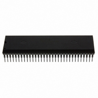
IC 10MHZ STATIC Z180 64-DIP
Manufacturer
Zilog
Datasheet
1.Z8S18010PSG.pdf
(71 pages)
Specifications of Z8S18010PSG
Processor Type
Z180
Features
Enhanced Z180
Speed
10MHz
Voltage
5V
Mounting Type
Through Hole
Package / Case
64-DIP (0.750", 19.05mm)
Processor Series
Z8S180X
Core
Z80
Data Bus Width
8 bit
Maximum Clock Frequency
10 MHz
Number Of Timers
2
Operating Supply Voltage
0 V to 3.3 V
Maximum Operating Temperature
+ 70 C
Mounting Style
Through Hole
Development Tools By Supplier
Z8S18000ZEM
Minimum Operating Temperature
0 C
Lead Free Status / RoHS Status
Lead free / RoHS Compliant
Other names
269-4297
Z8S18010PSG
Z8S18010PSG
Available stocks
Company
Part Number
Manufacturer
Quantity
Price
Company:

Part Number:
Z8S18010PSG
Manufacturer:
Zilog
Quantity:
48


stitute an 8-bit bidirectional data bus, used for the transfer
of information to and from I/O and memory devices. The
data bus enters the high-impedance state during reset and
external bus acknowledge cycles.
ZiLOG
20-bit address bus. The Address Bus provides the address
for memory data bus exchanges (up to 1 MB) and I/O data
bus exchanges (up to 64 KB). The address bus enters a
high–impedance state during reset and external bus ac-
knowledge cycles. Address line
output of PRT channel 1 (
on reset), and address line
sions of the Z8S180.
dress and data bus, and some control signals enter their high-
impedance state.
used by external devices (such as DMA controllers) to re-
quest access to the system bus. This request demands a high-
er priority than
the current machine cycle. This signal stops the CPU from
executing further instructions, places addresses, data buses,
and other control signals into the high-impedance state.
al). When in output mode, these pins are the transmit and
receive clock outputs from the ASCI baud rate generators.
When in input mode, these pins serve as the external clock
inputs for the ASCI baud rate generators.
plexed with
the CSI/O channel.
These lines are modem control signals for the ASCI chan-
nels.
grammable modem control signal for ASCI channel 0.
Low).
of the on-chip DMA channels. The DMA channels monitor
these inputs to determine when an external device is ready
for a
grammed to be either level or edge sensed.
tiplexed with
Serial Clock (bidirectional). This line is the clock for
. Data Carrier Detect 0 (Input, active Low); a pro-
Data Bus = (bidirectional, 3-state).
indicates that the requesting device, the MPU ad-
. Bus Acknowledge (Output, active Low).
Address Bus (Output, 3-state).
Bus Request (Input, active Low). This input is
is multiplexed with
or
. Clear to send 0 and 1 (Inputs, active Low).
is used to request a DMA transfer from one
Asynchronous Clock 0 and 1 (bidirection-
. DMA Request 0 and 1 (Input, active
, and
.
and is always recognized at the end of
operation. These inputs can be pro-
is multiplexed with
, selected as address output
is not available in DIP ver-
is multiplexed with the
.
is multi-
is mul-
form a
con-
.
nous, machine-cycle clock output during bus transactions.
connections. An external clock can be input to the
Z8S180/Z8L180 on this pin when a crystal is not used. This
input is Schmitt triggered.
asserted after the CPU executes either the
instruction and is waiting for either a nonmaskable or a
maskable interrupt before operation can resume. It is also
used with the
CPU machine cycle.
This signal is generated by external I/O devices. The CPU
honors these requests at the end of the current instruction
cycle as long as the
The CPU acknowledges this interrupt request with an in-
terrupt acknowledge cycle. During this cycle, both the
and
active Low). This signal is generated by external I/O de-
vices. The CPU honors these requests at the end of the cur-
rent instruction cycle as long as the
signals are inactive. The CPU acknowledges these requests
with an interrupt acknowledge cycle. Unlike the acknowl-
edgment for
active during this cycle.
dicates that the address bus contains a valid I/O address for
an
ated, along with
tor can be place onto the data bus. This signal is analogous
to the
fetch cycle of instruction execution. Together with
edgment. It is also used with the
code the status of the CPU machine cycle. This signal is
analogous to the
for a memory
nal is analogous to the
gered).
Enable Clock (Output). This pin functions as a synchro-
. Machine Cycle 1 (Output, active Low). Together with
indicates that the current cycle is for interrupt acknowl-
. Nonmaskable Interrupt (Input, negative edge trig-
. Maskable Interrupt Request 0 (Input, active Low).
. I/O Request (Output, active Low, 3-state).
input signal to indicate that an interrupt response vec-
.
,
. Memory Request (Output, active Low, 3-state).
indicates that the address bus holds a valid address
External Clock Crystal (Input). Crystal oscillator
signals become active.
signal of the Z64180.
. Maskable Interrupt Request 1 and 2 (Inputs,
indicates that the current cycle is the opcode-
demands a higher priority than
/
or
and
, neither the
or memory
signal of the Z64180.
, during the acknowledgment of the
(Output, active Low). This output is
and
signals to decode the status of the
signal of Z64180.
operation.
or
,
signals are inactive.
and
operation. This sig-
signals become
is also gener-
signal to de-
, and
or
and is al-
in-
,
Related parts for Z8S18010PSG
Image
Part Number
Description
Manufacturer
Datasheet
Request
R

Part Number:
Description:
Z8S180 APPLICATION BOARD
Manufacturer:
Zilog
Datasheet:

Part Number:
Description:
Communication Controllers, ZILOG INTELLIGENT PERIPHERAL CONTROLLER (ZIP)
Manufacturer:
Zilog, Inc.
Datasheet:

Part Number:
Description:
KIT DEV FOR Z8 ENCORE 16K TO 64K
Manufacturer:
Zilog
Datasheet:

Part Number:
Description:
KIT DEV Z8 ENCORE XP 28-PIN
Manufacturer:
Zilog
Datasheet:

Part Number:
Description:
DEV KIT FOR Z8 ENCORE 8K/4K
Manufacturer:
Zilog
Datasheet:

Part Number:
Description:
KIT DEV Z8 ENCORE XP 28-PIN
Manufacturer:
Zilog
Datasheet:
Part Number:
Description:
DEV KIT FOR Z8 ENCORE 4K TO 8K
Manufacturer:
Zilog
Datasheet:
Part Number:
Description:
CMOS Z8 microcontroller. ROM 16 Kbytes, RAM 256 bytes, speed 16 MHz, 32 lines I/O, 3.0V to 5.5V
Manufacturer:
Zilog, Inc.
Datasheet:
Part Number:
Description:
Low-cost microcontroller. 512 bytes ROM, 61 bytes RAM, 8 MHz
Manufacturer:
Zilog, Inc.
Datasheet:
Part Number:
Description:
Z8 4K OTP Microcontroller
Manufacturer:
Zilog, Inc.
Datasheet:
Part Number:
Description:
CMOS SUPER8 ROMLESS MCU
Manufacturer:
Zilog, Inc.
Datasheet:
Part Number:
Description:
SL1866 CMOSZ8 OTP Microcontroller
Manufacturer:
Zilog, Inc.
Datasheet:
Part Number:
Description:
SL1866 CMOSZ8 OTP Microcontroller
Manufacturer:
Zilog, Inc.
Datasheet:
Part Number:
Description:
OTP (KB) = 1, RAM = 125, Speed = 12, I/O = 14, 8-bit Timers = 2, Comm Interfaces Other Features = Por, LV Protect, Voltage = 4.5-5.5V
Manufacturer:
Zilog, Inc.
Datasheet: