Z8S18010PSG Zilog, Z8S18010PSG Datasheet - Page 12
Z8S18010PSG
Manufacturer Part Number
Z8S18010PSG
Description
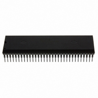
IC 10MHZ STATIC Z180 64-DIP
Manufacturer
Zilog
Datasheet
1.Z8S18010PSG.pdf
(71 pages)
Specifications of Z8S18010PSG
Processor Type
Z180
Features
Enhanced Z180
Speed
10MHz
Voltage
5V
Mounting Type
Through Hole
Package / Case
64-DIP (0.750", 19.05mm)
Processor Series
Z8S180X
Core
Z80
Data Bus Width
8 bit
Maximum Clock Frequency
10 MHz
Number Of Timers
2
Operating Supply Voltage
0 V to 3.3 V
Maximum Operating Temperature
+ 70 C
Mounting Style
Through Hole
Development Tools By Supplier
Z8S18000ZEM
Minimum Operating Temperature
0 C
Lead Free Status / RoHS Status
Lead free / RoHS Compliant
Other names
269-4297
Z8S18010PSG
Z8S18010PSG
Available stocks
Company
Part Number
Manufacturer
Quantity
Price
Company:

Part Number:
Z8S18010PSG
Manufacturer:
Zilog
Quantity:
48


ways recognized at the end of an instruction, regardless of
the state of the interrupt-enable flip-flops. This signal forces
CPU execution to continue at location
ence clock for the MPU and the external system. The fre-
quency of this output may be one-half, equal to, or twice
the crystal or input clock frequency.
the CPU wants to read data from either memory or an I/O
device. The addressed I/O or memory device should use this
signal to gate data onto the CPU data bus.
contents of the address bus should be used for refresh of dy-
namic memories. The low-order 8 bits of the address bus
(
to the REF signal of the Z64180.
mable MODEM control signal for ASCI channel 0.
are the receive data for the ASCI channels.
receive data for the CSI/O channel. RXS is multiplexed with
the
See Table 3.
Notes:
Status (Output). This signal is used with the
Read (Output, active Low, 3-state).
System Clock (Output). The output is used as a refer-
Clocked Serial Receive Data (Input). This line is the
indicates that the current CPU machine cycle and the
output to decode the status of the CPU machine cycle.
Refresh (Output, active Low). Together with
Request to Send 0 (Output, active Low); a program-
) contain the refresh address.
signal for ASCI channel 1.
Receive Data 0 and 1 (Input). These signals
This signal is analogous
0066H
indicates that
.
and
,
Low). This output is asserted active during the most recent
end of the block transfer.
and should be left open.
channel 1. This line is multiplexed with
bus.
nals are the transmitted data from the ASCI channels. Trans-
mitted data changes are with respect to the falling edge of
the transmit clock.
the transmitted data from the CSI/O channel.
MPU that the addressed memory or I/O devices are not
ready for data transfer. This input is sampled on the falling
edge of
sampled Low, then the additional
until the
cution continues.
the CPU data bus holds valid data to be stored at the ad-
dressed I/O or memory location.
should be left open if an external clock is used instead of a
crystal. The oscillator input is not a TTL level (see
acteristics).
Several pins are used for different conditions, depending on
the circumstance.
.
Clocked Serial Transmit Data (Output). This line is
. Wait (Input, active Low).
Timer Out (Output).
Test (Output, not in DIP version). This pin is for test
Crystal Oscillator Connection (Input). This pin
cycle of a DMA operation. It is used to indicate the
(and subsequent
(Output, active Low, 3-state).
Transmit Data 0 and 1 (Outputs). These sig-
input is sampled High, at which time exe-
Transfer End 0 and 1 (Outputs, active
is multiplexed with
is the output from PRT
states). If the input is
states are inserted
indicates to the
of the address
indicates that
DC Char-
ZiLOG
.
Related parts for Z8S18010PSG
Image
Part Number
Description
Manufacturer
Datasheet
Request
R

Part Number:
Description:
Z8S180 APPLICATION BOARD
Manufacturer:
Zilog
Datasheet:

Part Number:
Description:
Communication Controllers, ZILOG INTELLIGENT PERIPHERAL CONTROLLER (ZIP)
Manufacturer:
Zilog, Inc.
Datasheet:

Part Number:
Description:
KIT DEV FOR Z8 ENCORE 16K TO 64K
Manufacturer:
Zilog
Datasheet:

Part Number:
Description:
KIT DEV Z8 ENCORE XP 28-PIN
Manufacturer:
Zilog
Datasheet:

Part Number:
Description:
DEV KIT FOR Z8 ENCORE 8K/4K
Manufacturer:
Zilog
Datasheet:

Part Number:
Description:
KIT DEV Z8 ENCORE XP 28-PIN
Manufacturer:
Zilog
Datasheet:
Part Number:
Description:
DEV KIT FOR Z8 ENCORE 4K TO 8K
Manufacturer:
Zilog
Datasheet:
Part Number:
Description:
CMOS Z8 microcontroller. ROM 16 Kbytes, RAM 256 bytes, speed 16 MHz, 32 lines I/O, 3.0V to 5.5V
Manufacturer:
Zilog, Inc.
Datasheet:
Part Number:
Description:
Low-cost microcontroller. 512 bytes ROM, 61 bytes RAM, 8 MHz
Manufacturer:
Zilog, Inc.
Datasheet:
Part Number:
Description:
Z8 4K OTP Microcontroller
Manufacturer:
Zilog, Inc.
Datasheet:
Part Number:
Description:
CMOS SUPER8 ROMLESS MCU
Manufacturer:
Zilog, Inc.
Datasheet:
Part Number:
Description:
SL1866 CMOSZ8 OTP Microcontroller
Manufacturer:
Zilog, Inc.
Datasheet:
Part Number:
Description:
SL1866 CMOSZ8 OTP Microcontroller
Manufacturer:
Zilog, Inc.
Datasheet:
Part Number:
Description:
OTP (KB) = 1, RAM = 125, Speed = 12, I/O = 14, 8-bit Timers = 2, Comm Interfaces Other Features = Por, LV Protect, Voltage = 4.5-5.5V
Manufacturer:
Zilog, Inc.
Datasheet: