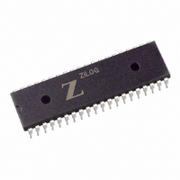
Z85C3010PSG Zilog, Z85C3010PSG Datasheet - Page 32

Z85C3010PSG
Manufacturer Part Number
Z85C3010PSG
Description
IC 10MHZ Z8500 CMOS SCC 40-DIP
Manufacturer
Zilog
Series
SCCr
Specifications of Z85C3010PSG
Processor Type
Z80
Features
Error Detection and Multiprotocol Support
Speed
10MHz
Voltage
5V
Mounting Type
Through Hole
Package / Case
40-DIP (0.620", 15.75mm)
Cpu Speed
8MHz
Digital Ic Case Style
DIP
No. Of Pins
40
Supply Voltage Range
5V
Operating Temperature Range
0°C To +70°C
Svhc
No SVHC (18-Jun-2010)
Base Number
85
Rohs Compliant
Yes
Clock Frequency
10MHz
Lead Free Status / RoHS Status
Lead free / RoHS Compliant
Other names
269-3934
Z85C3010PSG
Z85C3010PSG
Available stocks
Company
Part Number
Manufacturer
Quantity
Price
Company:
Part Number:
Z85C3010PSG
Manufacturer:
Zilog
Quantity:
135
Company:
Part Number:
Z85C3010PSG
Manufacturer:
Zilog
Quantity:
326
PS011705-0608
Z80C30
Z85C30/Z80C30 Setup
All SCC registers are directly addressable. A command issued in WR0B controls how the
SCC decodes the address placed on the address/data bus at the beginning of a Read or
Write cycle. In the Shift Right mode, the channel select A/B is taken from AD0 and the
state of AD5 is ignored. In the Shift Left mode, the channel select A/B is taken from AD5
and the state of AD0 is ignored. AD7 and AD6 are always ignored as address bits and the
register address occupies AD4-AD1.
Initialization
The system program first issues a series of commands to initialize the basic mode of
mode. For example, in the Asynchronous mode, character length, clock rate, number of
stop bits, and even or odd parity must be set first. The interrupt mode is set, and finally, the
receiver and transmitter are enabled.
Write Registers
The SCC contains 15 Write registers for the 80C30, while there are 16 for the 85C30 (one
more additional Write register if counting the transmit buffer) in each channel. These
Write registers are programmed separately to configure the functional ‘personality’ of the
channels. There are two registers (WR2 and WR9) shared by the two channels that are
accessed through either of them. WR2 contains the interrupt vector for both channels,
while WR9 contains the interrupt control bits and reset commands.
Figure 18
operation. This is followed by other commands to qualify conditions within the selected
display the format of each Write register.
CMOS SCC Serial Communications Controller
Product Specification
Figure 15
Functional Description
through
28


