MPC5200CVR400B Freescale Semiconductor, MPC5200CVR400B Datasheet - Page 20
MPC5200CVR400B
Manufacturer Part Number
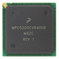
MPC5200CVR400B
Description
IC MPU 32BIT 400MHZ 272-PBGA
Manufacturer
Freescale Semiconductor
Specifications of MPC5200CVR400B
Processor Type
MPC52xx PowerPC 32-Bit
Speed
400MHz
Voltage
1.5V
Mounting Type
Surface Mount
Package / Case
272-PBGA
Processor Series
MPC52xx
Core
e300
Development Tools By Supplier
MEDIA5200KIT1E
Maximum Clock Frequency
400 MHz
Maximum Operating Temperature
+ 105 C
Mounting Style
SMD/SMT
I/o Voltage
2.5 V, 3.3 V
Minimum Operating Temperature
- 40 C
Core Size
32 Bit
No. Of I/o's
56
Ram Memory Size
16KB
Cpu Speed
400MHz
No. Of Timers
8
Embedded Interface Type
CAN, I2C, SCI, SPI
No. Of Pwm Channels
8
Digital Ic Case Style
TEPBGA
Rohs Compliant
Yes
Lead Free Status / RoHS Status
Lead free / RoHS Compliant
Features
-
Lead Free Status / Rohs Status
Lead free / RoHS Compliant
Available stocks
Company
Part Number
Manufacturer
Quantity
Price
Company:

Part Number:
MPC5200CVR400B
Manufacturer:
Marvell
Quantity:
1 001
Company:
Part Number:
MPC5200CVR400B
Manufacturer:
FREESCAL
Quantity:
200
Company:
Part Number:
MPC5200CVR400B
Manufacturer:
Freescale Semiconductor
Quantity:
10 000
Part Number:
MPC5200CVR400B
Manufacturer:
FREESCALE
Quantity:
20 000
Company:
Part Number:
MPC5200CVR400BM62C
Manufacturer:
FRRESCAL..
Quantity:
2 831


Electrical and Thermal Characteristics
3.3.5
3.3.5.1
3.3.5.2
In Standard SDRAM, all signals are activated on the Mem_clk from the Memory Controller and captured
on the Mem_clk clock at the memory device.
20
MBA (Bank Selects)
data
t
data
DQM (Data Mask)
DM
DM
mem_clk
Sym
t
t
valid
hold
Control Signals
valid
hold
setup
hold
MA (Address)
NOTE: Control Signals are composed of RAS, CAS, MEM_WE, MEM_CS, MEM_CS1 and CLK_EN
MDQ (Data)
MEM_CLK
SDRAM
MEM_CLK period
Control Signals, Address and MBA Valid after
rising edge of MEM_CLK
Control Signals, Address and MBA Hold after
rising edge of MEM_CLK
DQM valid after rising edge of MEM_CLK
DQM hold after rising edge of MEM_CLK
MDQ setup to rising edge of MEM_CLK
MDQ hold after rising edge of MEM_CLK
Memory Interface Timing-Standard SDRAM Read Command
Memory Interface Timing-Standard SDRAM Write Command
Figure 5. Timing Diagram—Standard SDRAM Memory Read Timing
t
t
t
valid
valid
valid
Description
Table 18. Standard SDRAM Memory Read Timing
Active
Row
t
hold
DM
valid
t
t
hold
hold
NOP
MPC5200 Data Sheet, Rev. 4
Column
READ
t
mem_clk
DM
t
mem_clk
NOP
data
hold
Min
7.5
0.2
—
—
—
*0.25-0.7
setup
*0.5
NOP
t
t
mem_clk
mem_clk
data
NOP
hold
Max
0.3
—
—
—
—
*0.25+0.4
*0.5+0.4
NOP
Freescale Semiconductor
Units
NOP
ns
ns
ns
ns
ns
ns
ns
SpecID
A5.1
A5.2
A5.3
A5.4
A5.5
A5.6
A5.7
Related parts for MPC5200CVR400B
Image
Part Number
Description
Manufacturer
Datasheet
Request
R

Part Number:
Description:
Manufacturer:
Freescale Semiconductor, Inc
Datasheet:
Part Number:
Description:
Manufacturer:
Freescale Semiconductor, Inc
Datasheet:
Part Number:
Description:
Manufacturer:
Freescale Semiconductor, Inc
Datasheet:
Part Number:
Description:
Manufacturer:
Freescale Semiconductor, Inc
Datasheet:
Part Number:
Description:
Manufacturer:
Freescale Semiconductor, Inc
Datasheet:
Part Number:
Description:
Manufacturer:
Freescale Semiconductor, Inc
Datasheet:
Part Number:
Description:
Manufacturer:
Freescale Semiconductor, Inc
Datasheet:
Part Number:
Description:
Manufacturer:
Freescale Semiconductor, Inc
Datasheet:
Part Number:
Description:
Manufacturer:
Freescale Semiconductor, Inc
Datasheet:
Part Number:
Description:
Manufacturer:
Freescale Semiconductor, Inc
Datasheet:
Part Number:
Description:
Manufacturer:
Freescale Semiconductor, Inc
Datasheet:
Part Number:
Description:
Manufacturer:
Freescale Semiconductor, Inc
Datasheet:
Part Number:
Description:
Manufacturer:
Freescale Semiconductor, Inc
Datasheet:
Part Number:
Description:
Manufacturer:
Freescale Semiconductor, Inc
Datasheet:
Part Number:
Description:
Manufacturer:
Freescale Semiconductor, Inc
Datasheet: