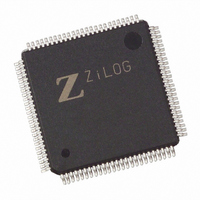
Z8018233ASG Zilog, Z8018233ASG Datasheet - Page 57

Z8018233ASG
Manufacturer Part Number
Z8018233ASG
Description
IC 33MHZ STATIC MIMIC 100-LQFP
Manufacturer
Zilog
Datasheet
1.Z8018233FSG.pdf
(109 pages)
Specifications of Z8018233ASG
Processor Type
Z180
Features
Smart Peripheral Controller
Speed
33MHz
Voltage
5V
Mounting Type
Surface Mount
Package / Case
100-LQFP
Processor Series
Z8018xx
Core
Z80
Data Bus Width
8 bit
Program Memory Type
ROMLess
Interface Type
UART
Maximum Clock Frequency
33 MHz
Number Of Programmable I/os
24
Number Of Timers
2
Operating Supply Voltage
4.5 V to 5.5 V
Maximum Operating Temperature
+ 70 C
Mounting Style
SMD/SMT
Minimum Operating Temperature
0 C
Lead Free Status / RoHS Status
Lead free / RoHS Compliant
Available stocks
Company
Part Number
Manufacturer
Quantity
Price
Z182 MISCELLANEOUS CONTROL AND INTERFACE REGISTERS
I/O And Memory Transactions
Z80182
/Z8L182
Data Bus
(DD
Z80182
/Z8L182
Data Bus
(DD
DS971820600
Figures 54 through 65 describe miscellaneous registers
that control the Z182 configuration, RAM/ROM chip select,
interrupt and various status and timers.
Zilog
D7 D6 D5 D4 D3 D2 D1 D0
0
OUT
OUT
0
Figure 54. System Configuration Register
=1)
=0)
(Z180 MPU Read/Write, Address xxEFH)
0
Peripherals
0
to On-Chip
I/O Write
0
Out
Out
0
0
From On-Chip
0
Peripherals
I/O Read
Out
Table 12a. Data Bus Direction (Z182 Bus Master)
Z
Daisy Chain
0=ESCC
1=16550 MIMIC> ESCC
ESCC/MIMIC
0=ESCC Channel B
1=16550 MIMIC Interface
Tri-Muxed Pins
0=Z80180
1=ESCC Channel/16550 MIMIC
Disable ROMs
0=ROM Sel Enabled
1=ROM Sel Disabled
DOUT
0=No Data Out
1=Data Out
Port PB4-PB0 Select
0=ASCI Channel 0 Func
1=PB4-PB0 Selected
Port PB7-PB5 Select
0=RXA1, TXA1, (RXS,/CTS1)
1=PB7-PB5 Selected
Port C Select
0=ESCC Channel A Func
1=Port C Selected
> 16550 MIMIC
P R E L I M I N A R Y
Peripherals
to Off-Chip
PS009801-0301
I/O Write
Out
Out
From Off-Chip
System Configuration Register
Bit 7 Port C Select
When this bit is set to 1, bit 8 parallel Port C is selected on
the multiplexed pins. When this bit is reset to 0 then these
multiplexed pins take ESCC
Bit 6 PB7-PB5 Select
When this bit is set to 1, parallel Port B bits 7 through 5 are
selected on the multiplexed pins. When this bit is reset to
0, these multiplexed pins become RxA1, TxA1 and RxS/
CTS1.
Bit 5 PB4-PB0 Select
When this bit is set to 1, parallel Port B bits 4 through 0 are
selected on the multiplexed pins. When this bit is reset to
0, these multiplexed pins take ASCI channel 0 functions.
Bit 4 DD
When this bit is set to 1, the Z182 is in “ROM emulator
mode”. In this mode, bus direction for certain transaction
periods are set to the opposite direction to export internal
bus transactions outside the Z80182/Z8L182. This allows
the use of ROM emulators/logic analyzers for application
development (see Tables 12a and 12b).
Note: The word “Out” means that the Z182 data bus
direction is in output mode, “In” means input mode, and “Z”
means high impedance. DD
Out and is the status of the D4 bit in the System Configuration
Register (SCR).
Peripherals
I/O Read
In
In
OUT
ROM Emulator Mode Enable
Memory
Write
Out
Out
To
Read
From
Mode
™
OUT
In
In
Channel A functions.
stands for Data Direction
Z
ILOG
Refresh Idle Mode
I
Z
NTELLIGENT
Z
Z80182/Z8L182
/Z8L182
P
Z80182
ERIPHERAL
Z
Z
3-57


