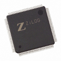
Z8018233ASG Zilog, Z8018233ASG Datasheet - Page 6

Z8018233ASG
Manufacturer Part Number
Z8018233ASG
Description
IC 33MHZ STATIC MIMIC 100-LQFP
Manufacturer
Zilog
Datasheet
1.Z8018233FSG.pdf
(109 pages)
Specifications of Z8018233ASG
Processor Type
Z180
Features
Smart Peripheral Controller
Speed
33MHz
Voltage
5V
Mounting Type
Surface Mount
Package / Case
100-LQFP
Processor Series
Z8018xx
Core
Z80
Data Bus Width
8 bit
Program Memory Type
ROMLess
Interface Type
UART
Maximum Clock Frequency
33 MHz
Number Of Programmable I/os
24
Number Of Timers
2
Operating Supply Voltage
4.5 V to 5.5 V
Maximum Operating Temperature
+ 70 C
Mounting Style
SMD/SMT
Minimum Operating Temperature
0 C
Lead Free Status / RoHS Status
Lead free / RoHS Compliant
Available stocks
Company
Part Number
Manufacturer
Quantity
Price
Zilog
Z180 CPU SIGNALS (Continued)
/NMI. Non-maskable interrupt (input, negative edge
triggered). /NMI has a higher priority than /INT and is
always recognized at the end of an instruction, regardless
of the state of the interrupt enable flip-flops. This signal
forces CPU execution to continue at location 0066H.
/INT0. Maskable Interrupt Request 0 (input/output active
Low). This signal is generated by external I/O devices. The
CPU will honor this request at the end of the current
instruction cycle as long as the /NMI and /BUSREQ signals
are inactive. The CPU acknowledges this interrupt request
with an interrupt acknowledge cycle. During this cycle,
both the /M1 and /IORQ signals become active. The
internal Z180 MPU’s /INT0 source is: /INT0 or ESCC or the
MIMIC. This input is level triggered. /INT0 is an open-drain
output, so you can connect other open-drain interrupts
onto the circuit in addition to haveing a pull-up to VCC.
Z180 MPU UART AND SIO SIGNALS
CKA0, CKA1. Asynchronous Clocks 0 and 1 (bi-directional,
active High). These pins are the transmit and receive
clocks for the synchronous channels. CKA0 is multiplexed
with /DREQ0 on the CKA0//DREQ0 pin. CKA1 is multiplexed
with /TEND0 on the CKA1//TEND0 pin.
CKS. Serial Clock (bi-directional, active High). This line is
clock for the CSIO channel and is multiplexed with the
ESCC signal (/W//REQB) and the 16550 MIMIC interface
signal /HTxRDY on the CKS//W//REQB//HTxRDY pin.
/DCD0. Data Carrier Detect 0 (input, active Low). This is a
programmable modem control signal for ASCI channel 0.
/DCD0 is multiplexed with the PB2 (parallel Port B, bit 2) on
the /DCD0/PB2 pin.
/RTS0. Request to Send 0 (output, active Low). This is a
programmable modem control signal for ASCI channel 0.
This pin is multiplexed with PB0 (parallel Port B, bit 0) on the
/RTS0/PB0 pin.
/CTS0. Clear to Send 0 (input, active Low). This line is a
modem control signal for the ASCI channel 0. This pin is
multiplexed with PB1 (parallel Port B, bit 1) on the /CTS0
/PB1 pin.
3-6
PS009801-0301
P R E L I M I N A R Y
/INT1, /INT2. Maskable Interrupt Requests 1 and 2 (inputs,
active Low). This signal is generated by external I/O
devices. The CPU will honor these requests at the end of
the current instruction cycle as long as the /NMI, /BUSREQ,
and /INT0 signals are inactive. The CPU acknowledges
these interrupt requests with an interrupt acknowledge
cycle. Unlike the acknowledgment for /INT0, during this
cycle neither the /M1 or /IORQ signals become active.
These pins may be programmed to provide an active Low
level on rising or falling edge interrupts. The level of the
external /INT1 and /INT2 pins may be read through bits
PC6 and PC7 of parallel Port C. Pin /INT1/PC6 multiplexes
/INT1 and PC6. Pin /INT2/PC7 multiplexes /INT2 and PC7.
/RFSH. Refresh (input/output, active Low, tri-state).
Together with /MREQ, /RFSH indicates that the current
CPU machine cycle and the contents of the address bus
should be used for refresh of dynamic memories. The low
order 8 bits of the address bus (A7-A0) contain the refresh
address. This signal is analogous to the /REF signal of the
Z64180.
TxA0. Transmit Data 0 (output, active High). This signal is
the transmitted data from the ASCI channel 0. This pin is
multiplexed with PB3 (parallel Port B, bit 3) on the
TxA0/PB3 pin.
TxS. Clocked Serial Transmit Data (output, active High) .
This line is the transmitted data from the CSIO channel. TxS
is multiplexed with the ESCC signal (/DTR//REQB) and the
16550 MIMIC interface signal HINTR on the TxS//DTR
//REQB//HINTR pin.
RxA0. Receive Data 0 (input, active High). This signal is
the receive data to ASCI channel 0. This pin is multiplexed
with PB4 (parallel Port B, bit 4) on the RxA0/PB4.
RxS. Clocked Serial Receive Data (input, active High).
This line is the receive data for the CSIO channel. RxS is
multiplexed with the /CTS1 signal for ASCI channel 1 and
with PB7 (parallel Port B, bit 7) on the RxS//CTS1/PB7 pin.
RxA1. Received Data ASCI channel 1 (input, active High).
This pin is multiplexed with PB6 (parallel Port B, bit 6) on the
RxA1/PB6 pin.
TxA1. Transmitted Data ASCI Channel 1 (output, active
High). This pin is multiplexed with PB5 (parallel Port B, bit
5) on the TxA1/PB5 pin.
Z
ILOG
I
NTELLIGENT
DS971820600
Z80182/Z8L182
P
ERIPHERAL


