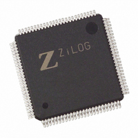
Z8018233ASG Zilog, Z8018233ASG Datasheet - Page 60

Z8018233ASG
Manufacturer Part Number
Z8018233ASG
Description
IC 33MHZ STATIC MIMIC 100-LQFP
Manufacturer
Zilog
Datasheet
1.Z8018233FSG.pdf
(109 pages)
Specifications of Z8018233ASG
Processor Type
Z180
Features
Smart Peripheral Controller
Speed
33MHz
Voltage
5V
Mounting Type
Surface Mount
Package / Case
100-LQFP
Processor Series
Z8018xx
Core
Z80
Data Bus Width
8 bit
Program Memory Type
ROMLess
Interface Type
UART
Maximum Clock Frequency
33 MHz
Number Of Programmable I/os
24
Number Of Timers
2
Operating Supply Voltage
4.5 V to 5.5 V
Maximum Operating Temperature
+ 70 C
Mounting Style
SMD/SMT
Minimum Operating Temperature
0 C
Lead Free Status / RoHS Status
Lead free / RoHS Compliant
Available stocks
Company
Part Number
Manufacturer
Quantity
Price
Zilog
RAMUBR, RAMLBR RAM Upper Boundary Range,
RAM Lower Boundary Range
These two registers specify the address range for the
/RAMCS signal. When accessed memory addresses are
less than or equal to the value programmed in the RAMUBR
and greater than or equal to the value programmed in the
RAMLBR, /RAMCS is asserted. The A18 signal from the
CPU is taken before it is multiplexed with T
that these registers are programmed to overlap,
/ROMCS takes priority over /RAMCS (/ROMCS is asserted
and /RAMCS is inactive).
Chip Select signals are going active for the address range:
/ROMCS: (ROMBR) >= A19-A12 >= 0
/RAMCS: (RAMUBR) >= A19-A12 >= (RAMLBR)
These registers are set to FFH at POR, and the boundary
addresses of ROM and RAM are as follows:
ROM lower boundary address
(fixed) = 00000H
ROM upper boundary address
(ROMBR register) = 0FFFFFH
RAM lower boundary address
(RAMLBR register) = 0FFFFFH
RAM upper boundary address
(RAMUBR register) = 0FFFFFH
A separate Wait State Generator is provided for access
memory using /ROMCS and /RAMCS. A single 8-bit register
is added to enable/disable this feature as well as provide
two 3-bit fields that provide 1 to 8 waits for each chip select.
WSG Chip Select Register (Z80182 address D8H)
3-60
/RAMCS AND /ROMCS REGISTERS (Continued)
Z80182 Improvement to the Wait State Generator
Bit 7
Bits 6-4
Bit 3
Bits 2-0
/RAMCS Wait State Generator Enable.
Disable on power-up or reset.
/RAMCS Wait States 1 to 8.
Eight wait states on power-up or reset.
/ROMCS Wait State Generator Enable.
Disable on power-up or reset.
/ROMCS Wait States 1 to 8.
Eight wait states on power-up or reset.
OUT
P R E L I M I N A R Y
. In the case
PS009801-0301
Because /ROMCS takes priority over /RAMCS, the latter
will never be asserted until the value in the ROMBR and
RAMLBR registers are re-initialized to lower values.
ROMBR ROM Address Boundary Register
This register specifies the address range for the /ROMCS
signal. When accessed, memory addresses are less than
or equal to the value programmed in this register, the
/ROMCS signal is asserted.
The A18 signal from the CPU is obtained before it is
multiplexed with T
(inactive state) by setting bit 3 in the System Configuration
Register, to allow the user to overlay the RAM area over the
ROM area.
There are two wait state generators in the Z182. The actual
number of wait states inserted is the greatest number of
both the Z180 WSG and the chip select WSG. In order to
use the Chip Select WSG, the Z180 WSG should be
programmed to 0 wait states.
Upon reset
(Z180 MPU Read/Write, Address xxE8H)
(Z180 MPU Read/Write, Address xxD8H)
D7 D6
Figure 58. WSG Chip Select Register
0
D7 D6 D5 D4 D3 D2 D1 D0
1
D5 D4 D3 D2 D1 D0
1
Figure 57. ROMBR
OUT
. This signal can be forced to a “1”
1
0
1
1
1
Z
ILOG
1
/ROMCS
Wait States
1-8
/ROMCS Wait
State Generator
Enable
/RAMCS Wait
States 1-8
/RAMCS Wait State
Generator Enable
I
NTELLIGENT
1
DS971820600
A19-A12
Z80182/Z8L182
P
ERIPHERAL


